
Phase shift mask, manufacturing method thereof and haze defect detection method thereof

A manufacturing method and mask plate technology, which are applied in the direction of photolithographic process exposure device, photographic process of pattern surface, semiconductor/solid-state device manufacturing, etc., can solve the problems of undetectable, labor-intensive, inaccurate detection, etc., and achieve The time is short, the cost is low, and the effect of online detection is realized

Active Publication Date: 2012-06-06
SEMICONDUCTOR MANUFACTURING INTERNATIONAL (BEIJING) CORP
View PDF6 Cites 13 Cited by
  • Summary
  • Abstract
  • Description
  • Claims
  • Application Information

AI Technical Summary

Problems solved by technology

This detection method takes a long time, requires a lot of manpower, and the detection is inaccurate. It cannot detect the repeated defects that appear before and after scanning the wafer.
[0009] The biggest defect of the above two methods is that the online monitoring of foggy defects cannot be realized. When the foggy defects are detected on the selected phase shift mask, the foggy defects may have already appeared, so that in the production of wafers The phase-shift mask with foggy defects may be used in the process, so the wafers produced have been affected by the foggy defects, that is, the existing methods are all off-line detection methods, which cannot be detected in time and accurately. Haze defects on the phase shift reticle cannot guarantee that the wafers produced before the detection of the haze defects on the phase shift reticle will not be affected by the haze defects

Method used


Image

  • Phase shift mask, manufacturing method thereof and haze defect detection method thereof
  • Phase shift mask, manufacturing method thereof and haze defect detection method thereof
  • Phase shift mask, manufacturing method thereof and haze defect detection method thereof

Examples


Embodiment Construction

[0066] In order to make the above objects, features and advantages of the present invention more comprehensible, specific implementations of the present invention will be described in detail below in conjunction with the accompanying drawings.

[0067] In the following description, many specific details are set forth in order to fully understand the present invention, but the present invention can also be implemented in other ways than those described here, so the present invention is not limited by the specific embodiments disclosed below.

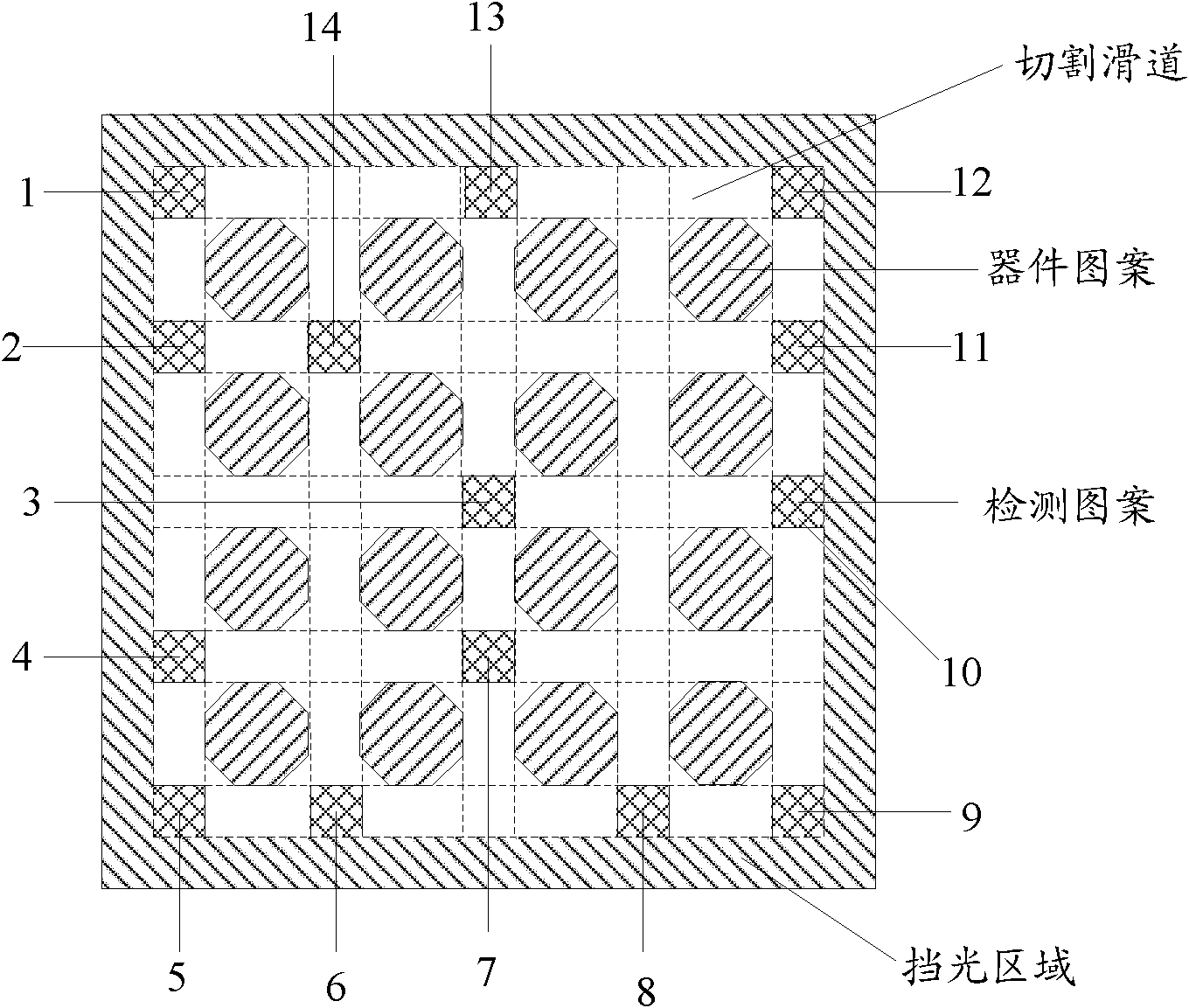
[0068] As mentioned in the background section, in the prior art, it takes a lot of time and manpower to detect the foggy defects on the phase shift reticle, and the detection accuracy is very low. More importantly, the existing detection methods are all offline detection, even if the foggy defect is detected, the foggy defect may already exist on the phase shift reticle before the foggy defect is detected.

[0069] Therefore, in order to ...


PUM


Abstract

The invention relates to a phase shift mask, a manufacturing method thereof and a haze defect detection method thereof in the technical field of semiconductors. The phase shift mask comprises a mask substrate, at least one cutting slide, a plurality of device patterns, at least one detection pattern, and a light blocking zone. The manufacturing method of the phase shift mask comprises the following steps: 1, preparing the mask substrate; 2, preparing the at least one detection pattern; 3, preparing the device patterns; and 4, manufacturing the light blocking zone. The haze defect detection method of the phase shift mask comprises the following steps: 1, exposing patterns on the phase shift mask to a photoresist layer of a wafer; 2, developing; 3, carrying out detect detection scanning on the wafer, and determining the phase shift mask is unqualified when haze defects appear on the detection pattern of the wafer and haze defects also appear on the device patterns of the wafer. According to the invention, the time for cleaning the phase shift mask can be timely and accurately determined, online detection is realized, the consumed time is short, and the cost is low.

Description

technical field [0001] The present invention relates to a device and method in the technical field of semiconductors, and in particular to a phase shift mask, a manufacturing method thereof, and a fog defect detection method. Background technique [0002] In the process of silicon wafer lithography using a phase-shift mask, when the phase-shift mask is irradiated by the laser of the lithography machine for a certain period of time, especially under the irradiation of a light source with a wavelength of 193nm or below 193nm, the phase-shift mask will appear So-called hazes are gradually generated. Haze defects appear in various forms, such as milky white powder defects on the quartz glass on the back of the phase shift mask, crystal-like snow flake defects on both sides of the chromium (Cr) or molybdenum silicon (MoSi) pattern lines, phase shift Crystallized salt on the surface of the protective film of the reticle, etc. These defects are harmful, and they may lead to a sig...

Claims


Application Information

Patent Timeline
Patent Type & Authority Applications(China)
IPC IPC(8): G03F1/26G03F1/44G03F7/20H01L21/66H01L21/02G01N21/956
Inventor 胡华勇张士健林益世
Owner SEMICONDUCTOR MANUFACTURING INTERNATIONAL (BEIJING) CORP
Features
  • Generate Ideas
  • Intellectual Property
  • Life Sciences
  • Materials
  • Tech Scout
  • Unparalleled Data Quality
  • Higher Quality Content
  • 60% Fewer Hallucinations
Learn More