

Phase shift mask, manufacturing method thereof and haze defect detection method thereof
A manufacturing method and a phase shift technology, which are applied to the exposure device of photoengraving process, the photoengraving process of pattern surface, and the manufacture of semiconductor/solid-state devices, etc. The effect of short time, online detection and low cost
- Summary
- Abstract
- Description
- Claims
- Application Information
AI Technical Summary
Problems solved by technology
Method used
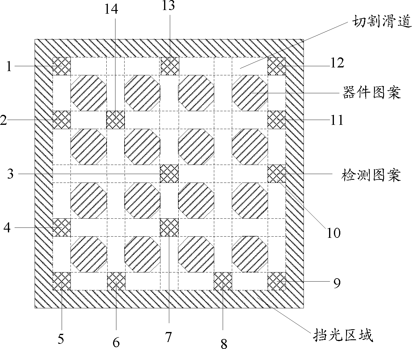
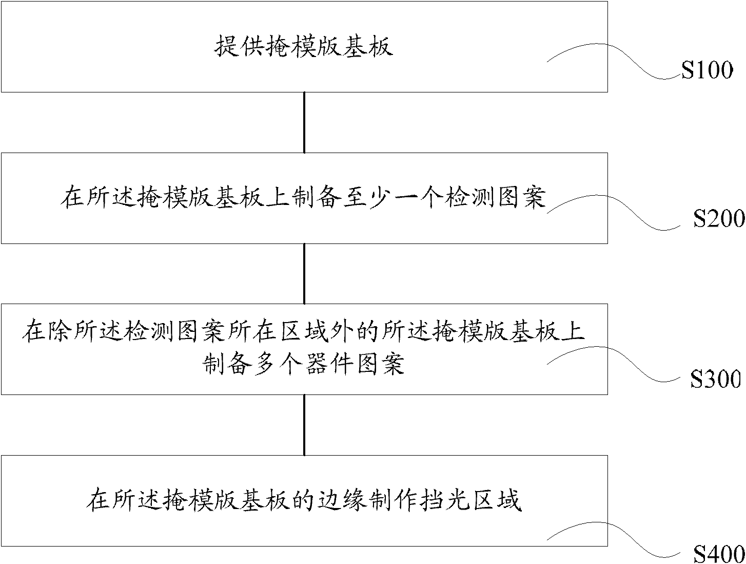
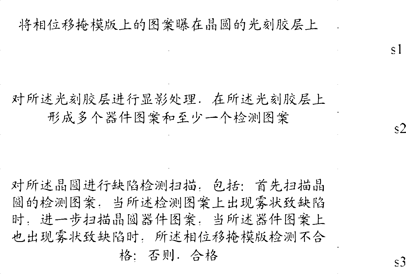
Image

Examples
Embodiment Construction
[0066] In order to make the above objects, features and advantages of the present invention more comprehensible, specific implementations of the present invention will be described in detail below in conjunction with the accompanying drawings.
[0067] In the following description, many specific details are set forth in order to fully understand the present invention, but the present invention can also be implemented in other ways than those described here, so the present invention is not limited by the specific embodiments disclosed below.
[0068] As mentioned in the background section, in the prior art, it takes a lot of time and manpower to detect the foggy defects on the phase shift reticle, and the detection accuracy is very low. More importantly, the existing detection methods are all offline detection, even if the foggy defect is detected, the foggy defect may already exist on the phase shift reticle before the foggy defect is detected.
[0069] Therefore, in order to ...
PUM
 Abstract
Description
Claims
Application Information