SOI/III-V full wafer bonding method adopting three-dimensional vent-hole device

A III-V, wafer bonding technology, used in electrical components, semiconductor/solid-state device manufacturing, circuits, etc., can solve the problems of dense bubbles at the interface, difficult to discharge gas, etc., to improve bonding strength, reduce material consumption, Density reduction effect

Active Publication Date: 2014-01-01
INST OF MICROELECTRONICS CHINESE ACAD OF SCI
View PDF2 Cites 0 Cited by
  • Summary
  • Abstract
  • Description
  • Claims
  • Application Information

AI Technical Summary

Problems solved by technology

[0007] In view of this, the main purpose of the present invention is to provide a SOI / III-V whole wafer bonding method using a three-dimensional vent device to solve the problem of bonding polymerization between interface atoms during direct bonding and post-processing. During the process, the gas will be difficult to discharge, and the problem of relatively dense bubble defects will be generated at the interface

Method used


Image

  • SOI/III-V full wafer bonding method adopting three-dimensional vent-hole device
  • SOI/III-V full wafer bonding method adopting three-dimensional vent-hole device
  • SOI/III-V full wafer bonding method adopting three-dimensional vent-hole device

Examples


Embodiment Construction

[0028] In order to make the object, technical solution and advantages of the present invention clearer, the present invention will be described in further detail below in conjunction with specific embodiments and with reference to the accompanying drawings.

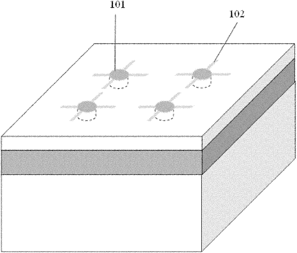
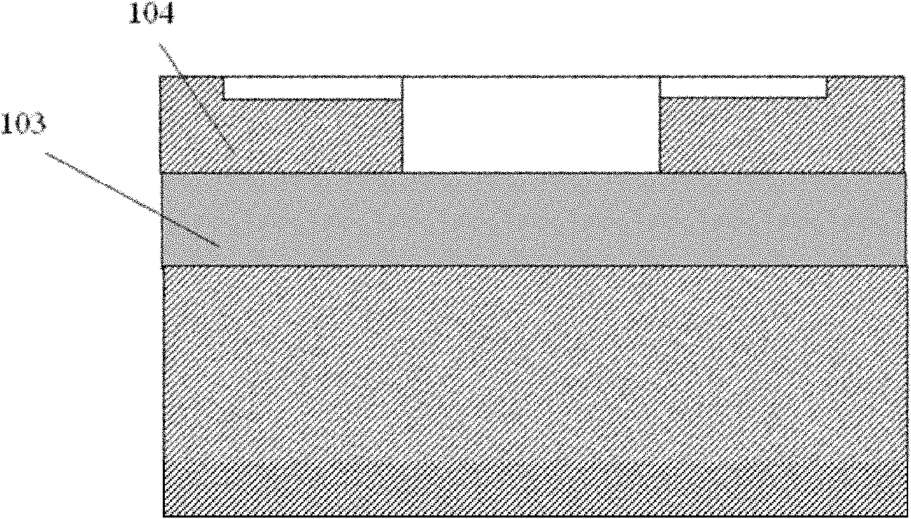
[0029] The embodiment of the present invention proposes a SOI / III-V whole wafer bonding technology using a three-dimensional vent device, figure 1 Shown is an appearance rendering of an SOI substrate with a three-dimensional vent structure, which includes vertical vent holes 103 and horizontal vent slots 104 . The exhaust hole is circular, and the aperture can be adjusted according to specific needs. The exhaust hole passes through the top Si layer of the SOI substrate to the BOX layer. The distance between the exhaust holes can be adjusted according to the specific application. It acts as a vertical exhaust channels that allow the H generated during the bonding process to 2 O and H 2 The gas is absorbed and diffused th...


PUM


Abstract

The invention discloses a SOI / III-V full wafer bonding method adopting a three-dimensional vent-hole device, belonging to the technical field of silicon-based photoelectric heterogeneous integration. The three-dimensional vent-hole device comprises two parts, namely a vertical vent hole and a horizontal vent groove, wherein the vertical vent hole is cylindrical, penetrates through top silicon and directly reaches a buried oxide layer; by arrangement of the vertical vent hole, H2O and H2 gas generated during the bonding process can be absorbed and diffused through the loose and porous buried oxide layer; and the horizontal vent groove is provided with a cross shallow slot concentric with the vent hole and serves as a horizontal ventilating device to collect gas so that the gas can be quickly and effectively absorbed and diffused through the vent hole. Through adoption of the three-dimensional vent-hole device, defects generated on a bonding interface because of bubbles can be reduced greatly and the wafer bonding quality can be effectively improved.

Description

technical field [0001] The invention relates to the technical field of silicon photoelectric heterogeneous integration, in particular to an SOI / III-V whole wafer bonding method using a three-dimensional exhaust hole device. Background technique [0002] Silicon-based microelectronics technology has been following Moore's law and has been developing continuously. The transistor integration density of microelectronic integrated circuits has increased rapidly, and the feature size has been continuously reduced. It has reached 22nm. There are insurmountable "bottlenecks" in terms of crosstalk, delay, and energy consumption, making the growth rate of information input and output capabilities unable to keep up with the growth of information processing capabilities. In order to continue Moore's Law, people in the industry continue to conduct research on new materials, new structures, and new devices. The development of silicon optoelectronics technology has brought new opportuniti...

Claims


Application Information

Patent Timeline
Patent Type & Authority Patents(China)
IPC IPC(8): H01L21/60H01L21/762H01L21/768
Inventor 刘新宇周静涛杨成樾刘焕明申华军吴德馨
Owner INST OF MICROELECTRONICS CHINESE ACAD OF SCI
Why Eureka
Try Eureka