Method of adhering flexible thin-film material to glass substrate

A flexible film material, glass substrate technology, applied in electrical components, semiconductor/solid-state device manufacturing, circuits, etc., to achieve the effects of good specificity, high yield and high viscosity

Inactive Publication Date: 2012-06-13
INST OF SEMICONDUCTORS - CHINESE ACAD OF SCI
View PDF2 Cites 5 Cited by
  • Summary
  • Abstract
  • Description
  • Claims
  • Application Information

AI Technical Summary

Problems solved by technology

[0005] The object of the present invention is to provide a kind of method that flexible thin film material is adhered on the glass substrate, in order to solve the flatness problem of operation substrate in the process of carrying out microelectronics process on the surface of flexible thin film material

Method used


Image

  • Method of adhering flexible thin-film material to glass substrate
  • Method of adhering flexible thin-film material to glass substrate
  • Method of adhering flexible thin-film material to glass substrate

Examples


Embodiment Construction

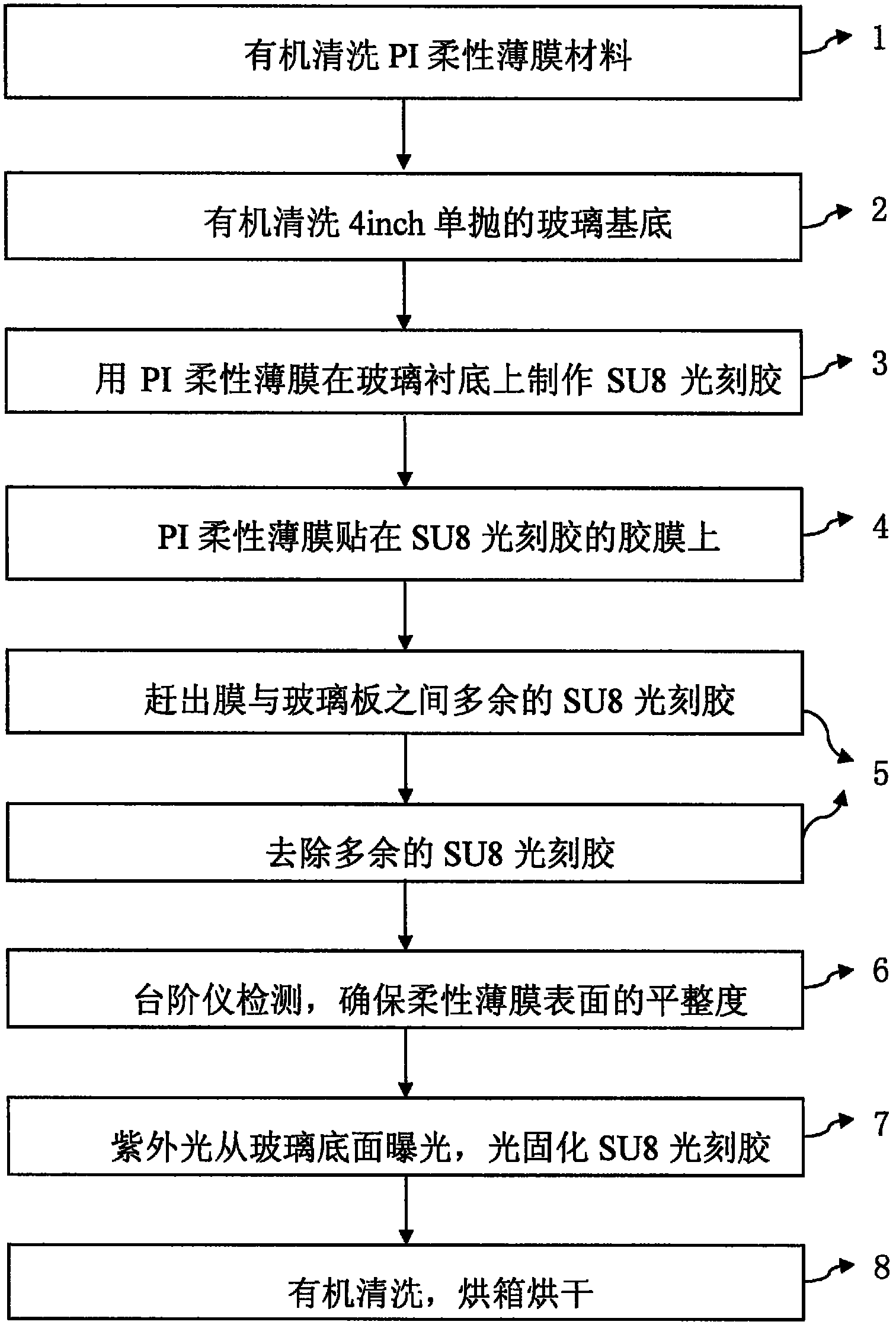
[0031] In order to make the object, technical solution and advantages of the present invention clearer, the present invention will be described in further detail below in conjunction with specific embodiments and with reference to the accompanying drawings.

[0032] Transferring the existing semiconductor process on inorganic materials to flexible film materials such as PI and PET is a shortcut to realize lightweight and flexible devices. Inorganic micro-nano processing technology has high requirements on the flatness of the substrate surface. Flexible thin film materials are soft and have poor surface flatness, making it difficult to directly fabricate devices on flexible thin film materials. The invention can not only realize the lightweight, bendable, and low-cost of inorganic devices, but also utilize the existing mature microelectronic technology to effectively compensate for the shortcomings of some organic processes, such as difficulty in organic processes and poor chara...


PUM


Abstract

The invention discloses a method of adhering a flexible thin-film material to a glass substrate, which includes step 1: washing the glass substrate and the flexible thin-film material, step 2: adding SU8 photoresist to the glass substrate dropwise, step 3: leading one side of the flexible thin-film material to be contacted with the SU8 photoresist and flattening the flexible thin-film material from one side to the other side, step 4: extruding the flexible thin-film material by aid of a flat surface, extruding out redundant SU8 photoresist and wiping the redundant SU8 photoresist by aid of acetone, step 5: leading the back side of the glass substrate to be exposed by aid of ultraviolet light, and step 6: washing and drying the glass substrate. The method of adhering the flexible thin-film material to the glass substrate solves the problem of flatness of the operation substrate during microelectronics technology processing on the surface of the flexible thin-film material.

Description

technical field [0001] The invention relates to the field of micro-nano processing technology, in particular to a method for adhering a flexible film material on a glass substrate, which can be applied to the surface of a flexible film material: depositing metal films such as Al and Au, making flexible solar cells, flexible LED display and lighting, etc. are made of SiO 2 , SiN x Experiment and production of substrate flexibility for integrated devices such as microelectronics and optoelectronic devices. Background technique [0002] Polyimide (PI) is made of pyromellitic dianhydride (PMDA) and diaminodiphenyl ether (ODA) in a very strong solvent dimethylacetamide (DMAC) through polycondensation and salivation to form a film, and then through imidized. It is currently the best thin film insulating material in the world, with excellent mechanical properties, electrical properties, chemical stability, high radiation resistance, high temperature resistance and low temperatur...

Claims


Application Information

Patent Timeline
Patent Type & Authority Applications(China)
IPC IPC(8): H01L21/02
Inventor 付英春王晓峰王晓东杨富华
Owner INST OF SEMICONDUCTORS - CHINESE ACAD OF SCI
Why Eureka
Try Eureka