Method for preparing high-purity tantalum target

A tantalum target, high-purity technology, applied in the field of high-purity tantalum target preparation, can solve the problems of high resistivity, slow sputtering speed, unevenness, etc.

Active Publication Date: 2012-06-27
KONFOONG MATERIALS INTERNATIONAL CO LTD
View PDF1 Cites 38 Cited by
  • Summary
  • Abstract
  • Description
  • Claims
  • Application Information

AI Technical Summary

Problems solved by technology

This product is applied to the sputtering target, the sputtering speed is slow, and the tantalum film on the silicon wafer is tested after sputtering, and the resistivity is high or uneven

Method used


Image

  • Method for preparing high-purity tantalum target
  • Method for preparing high-purity tantalum target
  • Method for preparing high-purity tantalum target

Examples


Embodiment Construction

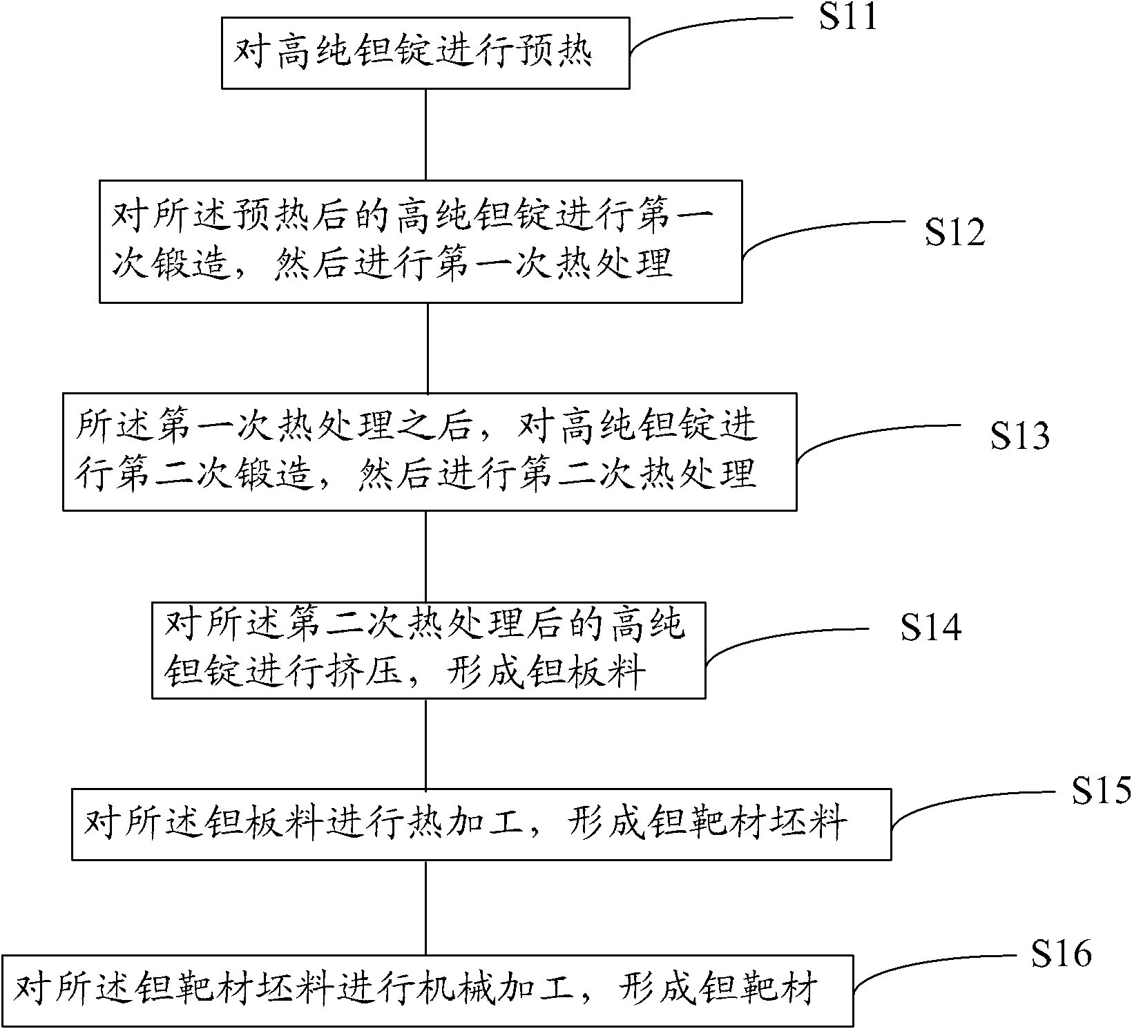
[0062]The present invention mainly realizes the production of tantalum target crystal grains for semiconductor sputtering by controlling the deformation rate of plastic deformation, the temperature and time of heat treatment, and combining the plastic deformation with specific deformation rate and heat treatment at a specific temperature for multiple times. Tantalum target material according to the requirements and crystal orientation requirements.

[0063] After the inventor's painstaking research and many practical improvements, the optimal method for making tantalum targets has been obtained, such as figure 1 As shown, it mainly includes the following steps:

[0064] Step S11, preheating the high-purity tantalum ingot;

[0065] Step S12, performing the first forging on the preheated high-purity tantalum ingot, and then performing the first heat treatment;

[0066] Step S13, after the first heat treatment, the high-purity tantalum ingot is forged for the second time, and t...


PUM

PropertyMeasurementUnit
particle sizeaaaaaaaaaa
diameteraaaaaaaaaa
heightaaaaaaaaaa

Abstract

A method for preparing a high-purity tantalum target comprises the following steps: preheating high-purity tantalum ingots; forging the preheated high-purity tantalum ingots by at least two times, wherein the high-purity tantalum ingots are heated after being forged each time; extruding the high-purity tantalum ingots after the high-purity tantalum ingots are heated for the last time, so as to obtain a tantalum board; heating the tantalum board to obtain a tantalum target blank; and machining the tantalum target blank to obtain the tantalum target. According to the process for preparing the tantalum target, the uniformity and the compactability of the tantalum target can be better, so as to meet the crystal particle requirements and the crystal orientation requirements of the tantalum target for semi-conductor sputtering.

Description

technical field [0001] The invention relates to the field of semiconductor sputtering, in particular to a method for preparing a high-purity tantalum target. Background technique [0002] The sputtering target is an extremely important key material necessary for the manufacture of semiconductor chips. The principle is to use physical vapor deposition technology (PVD) to bombard the target with high-pressure accelerated gaseous ions, so that the atoms of the target are sputtered out to It is deposited on the silicon wafer in the form of a thin film, which eventually forms the complex wiring structure in the semiconductor chip. Sputtering targets have many advantages such as uniformity and controllability of metal coatings, and are widely used in the semiconductor field. With the rapid development of the semiconductor industry, the demand for sputtering targets is increasing, and sputtering targets have become an indispensable key material for the development of the semicondu...

Claims


Application Information

Patent Timeline
Patent Type & Authority Applications(China)
IPC IPC(8): C22F1/18C23C14/34C23C14/14
Inventor 姚力军相原俊夫大岩一彦潘杰王学泽周友平
Owner KONFOONG MATERIALS INTERNATIONAL CO LTD
Why Eureka
Try Eureka