Process for photoetching polyimide on semiconductor substrate

A polyimide and semiconductor technology, which is applied in the field of semiconductor substrate processing technology, can solve the problems of silicon wafer rework, scrapping, insoluble developer solution, etc., and achieves the effect of reducing production time and manufacturing cost.

Inactive Publication Date: 2012-07-04
ADVANCED SEMICON MFG CO LTD
View PDF3 Cites 6 Cited by
  • Summary
  • Abstract
  • Description
  • Claims
  • Application Information

AI Technical Summary

Problems solved by technology

[0004] like figure 2 As shown, in the existing silicon wafer pretreatment process, after EKC wet stripping, the photoresist and other polymers on the surface of the passivation layer are not completely removed. Therefore, there is often a residue on the surface of the passivation layer A by-product that cannot be seen by visual inspection, this by-product will react with the polyimide in the subsequent polyimide lithography process to produce polyimide residues that cannot be dissolved by the developer 101, resulting in silicon Chip Rework or Scrap

Method used


Image

  • Process for photoetching polyimide on semiconductor substrate
  • Process for photoetching polyimide on semiconductor substrate
  • Process for photoetching polyimide on semiconductor substrate

Examples


Embodiment Construction

[0026] The semiconductor substrate polyimide process proposed by the present invention will be further described in detail below in conjunction with the accompanying drawings and specific embodiments.

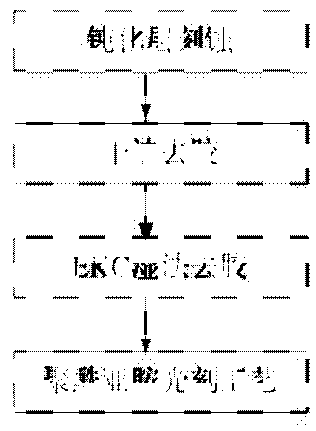
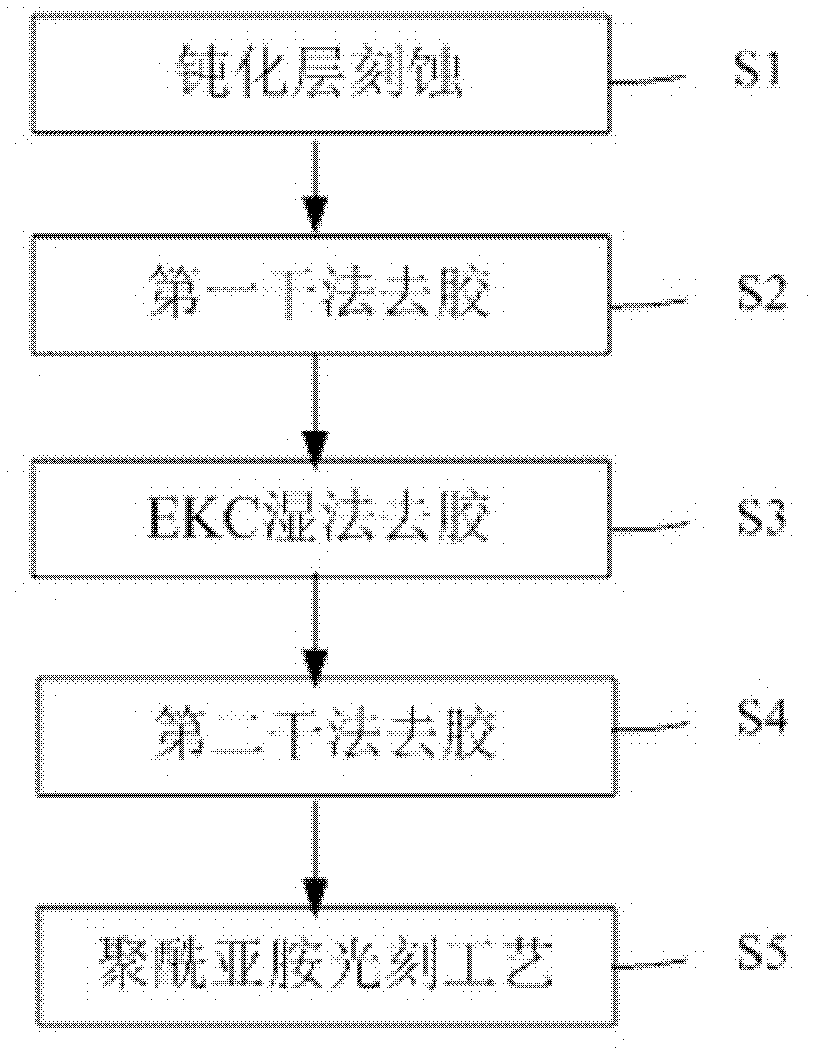
[0027] Such as image 3 Shown, the present invention provides a kind of semiconductor substrate polyimide process, comprises the following steps:

[0028] S1, etching the passivation layer on the semiconductor substrate;

[0029] S2, performing a first dry deglue on the semiconductor substrate;

[0030] S3, performing wet deglue on the semiconductor substrate;

[0031] S4, performing a second dry deglue on the semiconductor substrate;

[0032] S5, performing a polyimide photolithography process on the semiconductor substrate.

[0033] The semiconductor substrate described in the present invention can be a silicon wafer or other materials.

[0034] In step S1, the passivation layer may be silicon dioxide, silicon nitride, aluminum oxide, etc., used to block mobile ions, wat...


PUM


Abstract

The invention provides a process for photoetching polyimide on a semiconductor substrate. A one-step dry method for glue removal is added after a wet method for glue removal is performed; plasma gas can thoroughly remove residual byproducts from the surface of a passivation layer, so that a good effect that a polyimide residue is eliminated after development is performed by using a polyimide photoetching process is achieved; and therefore, an aim of zero reworking of a product in the step is fulfilled, the production time of the product is reduced, and the manufacturing cost is saved.

Description

technical field [0001] The invention relates to the technical field of semiconductor integrated circuit manufacturing technology, in particular to a semiconductor substrate processing technology. Background technique [0002] Polyimide (Polyimide, PI) is a kind of polymer material, which has the characteristics of high temperature resistance, radiation resistance, good insulation performance, corrosion resistance and stable chemical properties. material, but due to its special chemical properties, it has relatively high requirements for the cleanliness of the surface of the object. [0003] Such as figure 1 As shown, the existing silicon wafer pretreatment process is generally as follows: firstly, the passivation layer is etched on the silicon wafer; then, dry stripping and EKC wet stripping are performed in sequence, and then the polyimide photolithography process is performed. . [0004] Such as figure 2 As shown, in the existing silicon wafer pretreatment process, af...

Claims


Application Information

Patent Timeline
Patent Type & Authority Applications(China)
IPC IPC(8): H01L21/027
Inventor 吴正泉李鹏
Owner ADVANCED SEMICON MFG CO LTD
Why Eureka
Try Eureka