Opening filling method

A filling method and mask layer technology, applied in semiconductor/solid-state device components, vacuum evaporation plating, coating, etc., to achieve the effects of improving reliability, avoiding necking, and eliminating the probability of void defects

Active Publication Date: 2012-07-04
INST OF MICROELECTRONICS CHINESE ACAD OF SCI
View PDF3 Cites 6 Cited by
  • Summary
  • Abstract
  • Description
  • Claims
  • Application Information

AI Technical Summary

Problems solved by technology

[0006] In addition, through-holes used in 3D packaging and trenches in advanced metal interconnect processes, due to their large aspect ratio, lock-necks in the deposition of diffusion barrier and copper seed layers can also cause the same fill problem

Method used


Image

  • Opening filling method
  • Opening filling method
  • Opening filling method

Examples


Embodiment 1

[0036] Figure 5 It is a flow chart of the filling method of the opening in the present embodiment, Figure 6 to Figure 11 It is a schematic diagram of the opening filling method in this embodiment. In this embodiment, the process of filling via holes between metal wiring layers is taken as an example, and the openings are via holes.

[0037] As shown, the method of filling the opening includes:

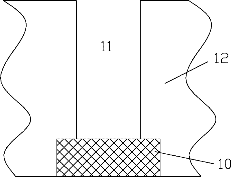
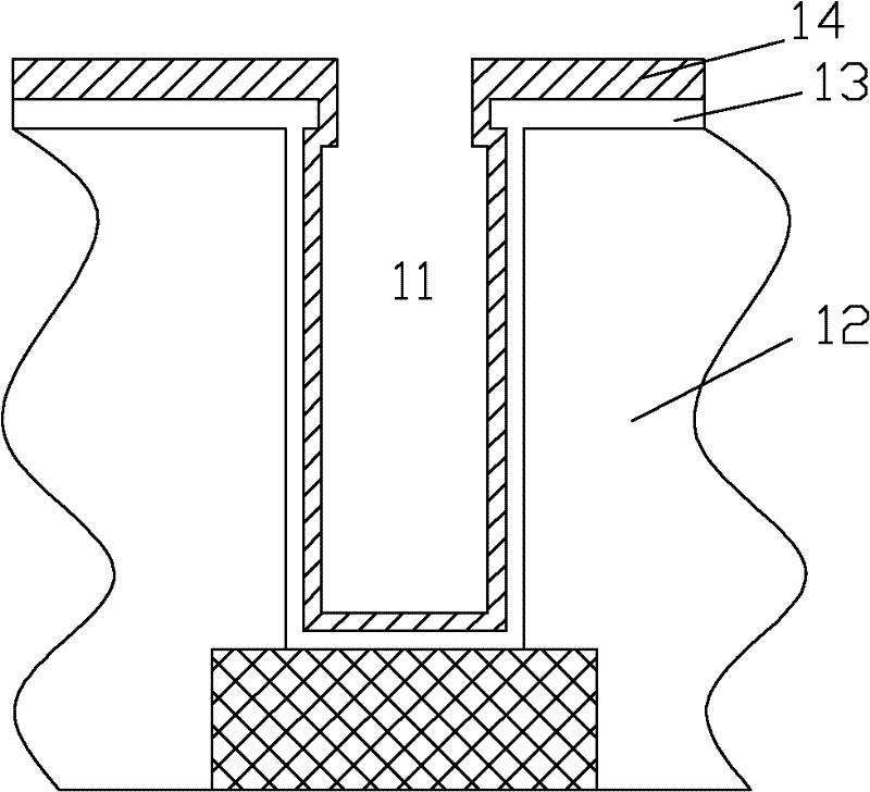
[0038] Step S1: Provide a semiconductor substrate, refer to Figure 6 As shown, the semiconductor substrate has at least an underlying metal wiring layer 101 and an isolation dielectric layer 102 above the underlying metal wiring layer 101 , and the isolation dielectric layer 102 has a through hole 103 therein. Here, the "bottom layer" is only relative to the metal wiring layer above it, and does not represent the first metal wiring layer. The semiconductor substrate also includes logic devices, power devices and / or storage devices (not shown in the figure), etc., which are locat...

Embodiment 2

[0060] Figure 13 It is a schematic diagram of the opening filling method in this embodiment. The filling method of described opening comprises:

[0061] A semiconductor substrate is provided, having at least an underlying metal wiring layer and an isolation dielectric layer above the underlying metal wiring layer, and an opening is provided in the isolation dielectric layer;

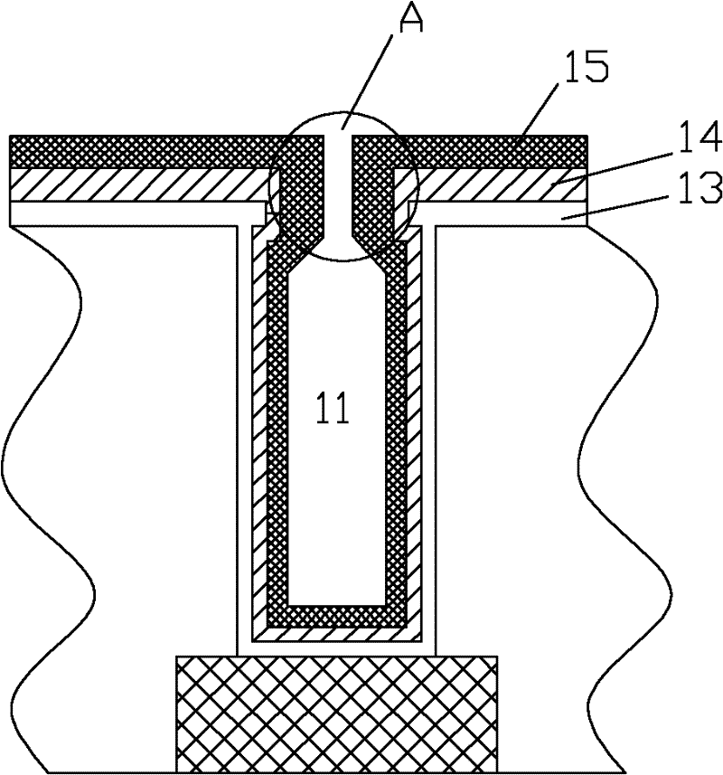
[0062] sequentially forming a diffusion barrier layer and a seed layer on the surface of the isolation medium layer inside and outside the opening;

[0063] forming a mask layer on the surface of the seed layer outside the opening;

[0064] Covering a metal layer on the semiconductor substrate with a mask layer, the metal layer filling the opening;

[0065] The planarization process is performed to remove the metal layer, the seed layer and the diffusion barrier layer outside the opening, so as to form a metal wiring layer.

[0066] The difference from the embodiment in the above steps is, as Figu...


PUM


Abstract

The invention provides an opening filling method, which includes: providing a semiconductor substrate at least comprising an underlying metal wire layer and an isolation dielectric layer above the underlying metal wire layer, wherein an opening is arranged in the isolation dielectric layer; sequentially forming diffusion barrier layers and seed layers on the surface of the isolation dielectric layer inside the opening and outside the opening; forming a mask layer on the surface of each seed layer outside the opening; and covering a metallic layer on the semiconductor substrate with the mask layers, and filling the opening with the metallic layer. As the diffusion barrier layers and the seed layers are sequentially formed on the surface of the isolation dielectric layer inside the opening and outside the opening, and the mask layers are formed on the surfaces of the seed layers outside the opening, under the barrier action of the mask layers, in the follow-up process of depositing the metallic layer on the semiconductor substrate, the metallic layer is not deposited on the surface inside and outside the opening simultaneously but is used for filling the inside of the opening firstly prior to depositing on the outer surface of the opening. Therefore, necking can be avoided, probability of void defects is decreased or eliminated, and reliability of circuits is enhanced.

Description

technical field [0001] The invention relates to the technical field of semiconductor manufacturing, in particular to an opening filling method. Background technique [0002] With the increasing demand for high integration and high performance of ultra-large-scale integrated circuits, semiconductor technology is developing towards technology nodes with 22nm or even smaller feature sizes, and the computing speed of chips is obviously affected by the resistance capacitance delay (Resistance Capacitance) Delay Time, RC Delay Time). Therefore, in the current semiconductor manufacturing technology, copper metal interconnection with lower resistivity is used to replace the traditional aluminum metal interconnection, so as to improve the phenomenon of RC delay. [0003] The copper electroplating process has been widely used in the metal interconnection manufacturing process of integrated circuits to fill the trenches and through holes in the dielectric layer, manufacture copper met...

Claims


Application Information

Patent Timeline
Patent Type & Authority Applications(China)
IPC IPC(8): H01L21/768H01L21/3205C23C14/14C23C14/06
CPCH01L21/76873H01L21/76898H01L21/76879H01L23/53238H01L21/76859H01L2924/0002H01L2924/00
Inventor 赵超王文武钟汇才
Owner INST OF MICROELECTRONICS CHINESE ACAD OF SCI
Why Eureka
Try Eureka