Semiconductor device and manufacturing method thereof

A manufacturing method and semiconductor technology, which are applied in the fields of semiconductor devices, semiconductor/solid-state device manufacturing, semiconductor/solid-state device parts, etc., can solve the problems of contamination, chemical reagent damage, affecting the dielectric constant of the first dielectric layer 110, and the like, Achieve the effect of avoiding metal contamination and preventing changes in dielectric constant

Active Publication Date: 2012-07-04
SEMICONDUCTOR MANUFACTURING INTERNATIONAL (BEIJING) CORP +1
View PDF4 Cites 8 Cited by
  • Summary
  • Abstract
  • Description
  • Claims
  • Application Information

AI Technical Summary

Problems solved by technology

Since the surface of the first dielectric layer 110 is exposed when the first metal cap layer 140 is formed, the chemical reagent used in the electroless deposition process will also damage the first dielectric layer 110, and it is very easy to Metal contamination is formed on the surface of the dielectric layer 110, thereby affecting...

Method used


Image

  • Semiconductor device and manufacturing method thereof
  • Semiconductor device and manufacturing method thereof
  • Semiconductor device and manufacturing method thereof

Examples


Embodiment Construction

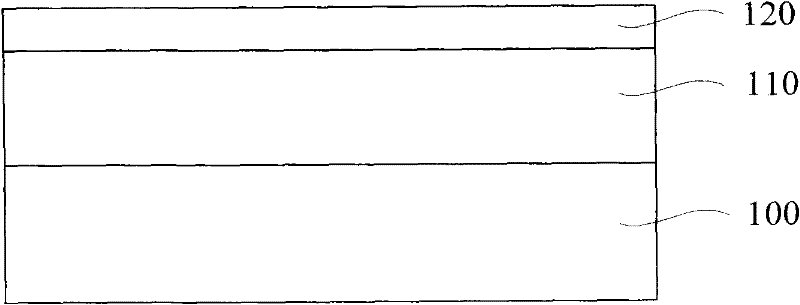
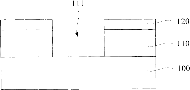
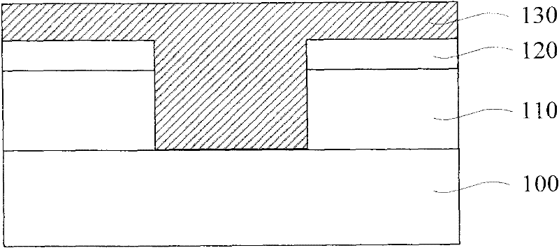
[0031] As mentioned in the background art, when the chemical mechanical polishing process is performed, the polishing liquid used will cause the dielectric constant of the first dielectric layer to change, which will adversely affect the performance of the subsequently formed metal interconnection lines. Therefore, the present invention covers the first barrier layer on the surface of the first dielectric layer, and only removes the first hard mask layer and part of the first metal layer when performing the first chemical mechanical polishing process, while retaining part or all of the The first barrier layer, that is, the surface of the first dielectric layer will not be exposed, therefore, the grinding liquid will not damage the first dielectric layer, which can prevent the dielectric constant of the first dielectric layer from changing; secondly, the first dielectric layer A barrier layer can also prevent the chemical reagent used when forming the first metal cap layer from ...


PUM


Abstract

The invention discloses a semiconductor device and a manufacturing method thereof. The manufacturing method of the semiconductor device comprises the following steps of: forming a first medium layer, a first barrier layer and a first hard mask layer in sequence on the surface of a semiconductor substrate; etching the first hard mask layer, the first barrier layer and the first medium layer to form a first groove; forming first metal layers in the first groove and on the surface of the first hard mask layer; and performing a first chemical-mechanical grinding process, removing the first hard mask layer and a part of the first metal layers, and keeping a part of or all of the first barrel layer to form a first metal interconnection line. The first barrier layer is formed, so that the dielectric coefficient of the first medium layer can be prevented from varying, and the reliability of the semiconductor device is enhanced.

Description

technical field [0001] The invention relates to the field of integrated circuit manufacturing, in particular to a semiconductor device and a manufacturing method thereof. Background technique [0002] At present, the manufacturing technology of semiconductor devices is developing rapidly, semiconductor devices already have a deep submicron structure, and integrated circuits contain a huge number of semiconductor elements. With the further development of semiconductor device manufacturing technology, high-performance, high-density connections between semiconductor devices are not only performed in a single interconnection layer, but also interconnected between multiple layers. Therefore, a multilayer metal interconnection structure is generally provided in which a plurality of interconnection layers are stacked on each other with a dielectric layer interposed therebetween for connecting semiconductor devices. Generally speaking, a dielectric film with a dielectric constant (...

Claims


Application Information

Patent Timeline
IPC IPC(8): H01L21/768H01L23/522H01L23/528
Inventor 胡敏达周俊卿张海洋
Owner SEMICONDUCTOR MANUFACTURING INTERNATIONAL (BEIJING) CORP
Why Eureka
Try Eureka