Method for improving erasing speed of SONOS (Silicon Oxide Nitride Oxide Silicon) by utilizing strained silicon technology

A technology of erasing and writing speed and strained silicon, which is applied in the manufacturing of electrical components, electric solid-state devices, semiconductor/solid-state devices, etc., can solve the problem of low hot electron injection programming efficiency, etc., to improve programming efficiency and speed, energy valley scattering probability The effect of reducing, reducing the effective mass

Active Publication Date: 2014-07-02
SHANGHAI HUALI MICROELECTRONICS CORP
View PDF6 Cites 0 Cited by
  • Summary
  • Abstract
  • Description
  • Claims
  • Application Information

AI Technical Summary

Problems solved by technology

When some electrons get enough high energy, hot electron injection occurs, but since only a small part of the channel is effective for programming, hot electron injection programming is not efficient

Method used


Image

  • Method for improving erasing speed of SONOS (Silicon Oxide Nitride Oxide Silicon) by utilizing strained silicon technology
  • Method for improving erasing speed of SONOS (Silicon Oxide Nitride Oxide Silicon) by utilizing strained silicon technology
  • Method for improving erasing speed of SONOS (Silicon Oxide Nitride Oxide Silicon) by utilizing strained silicon technology

Examples


Embodiment Construction

[0024] The present invention will be described in further detail below in conjunction with the accompanying drawings and specific embodiments. The specific embodiments described here are only used to explain the present invention, and are not used to limit the protection scope of the present invention.

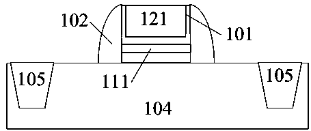
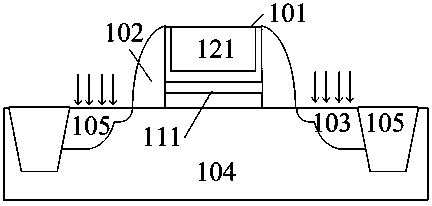
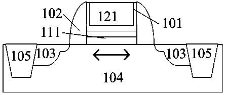
[0025] combined reference figure 1 and figure 2 , revealing the method of the present invention to improve the erasing and writing speed of SONOS by utilizing the strained silicon technology, figure 1 In the process, after forming the sidewall 102 of the gate 101 on the P-type substrate 104 with several shallow trench isolation regions 105 formed, the following steps are also included:

[0026] Step 1, precipitation barrier layer ( figure 1 not shown) covering the transistor;

[0027] Step 2, etch and remove the barrier layer covering the NMOS region to expose the NMOS region. In this step, first spin-coat photoresist on the barrier layer, and then perform photolithograph...


PUM


Abstract

The invention discloses a method for improving an erasing speed of an SONOS (Silicon Oxide Nitride Oxide Silicon) by utilizing a strained silicon technology. The method is characterized by comprising the following steps of: after manufacturing a sidewall of a grid electrode on a P-type substrate forming a plurality of shallow channel isolation regions, (1) depositing a baffle layer to cover a transistor; (2) etching to remove the baffle layer covering above an NMOS (N-channel Metal Oxide Semiconductor) region to expose the NMOS region; (3) etching silicon of active regions on two sides of the grid electrode of the NMOS region; (4) depositing silicon carbide at the active regions through a selectivity epitaxy process; and (5) carrying out high-temperature annealing to enable the silicon carbide to generate tensile stress on a channel. According to the method for increasing the erasing speed of the SONOS by utilizing the strained silicon technology, disclosed by the invention, an energy band of silicon is broken up so that effective mass of electron in the direction of the channel is reduced; simultaneously, energy valley scattering probability of the electron is also reduced, and mobility of the electron of the SONOS unit transistor is remarkably improved, thus the SONOS programming efficiency and speed of a hot electron injection mechanism are improved.

Description

technical field [0001] The invention relates to a silicon-silicon oxide-silicon nitride-silicon oxide-silicon (SONOS) memory, in particular to a method for improving the erasing and writing speed of the SONOS by utilizing strained silicon technology. Background technique [0002] The basic working principle of non-volatile semiconductor memory is to store charge in the gate dielectric of a MOSFET. Devices in which charges are stored in discrete trapping centers in a suitable dielectric layer are called charge-trapping devices. The most common of these devices is silicon-silicon oxide-nitride-silicon oxide-silicon (SONOS) memory. [0003] The main two storage mechanisms for storing data in flash memory cells are channel hot electron (CHE) injection and F-N tunneling. Channel hot electron injection is considered to be quite reliable after long-term cycling because it does not place significant stress on the tunnel oxide. But the disadvantage of CHE is that the programming e...

Claims


Application Information

Patent Timeline
Patent Type & Authority Patents(China)
IPC IPC(8): H01L21/8247H01L27/115
Inventor 葛洪涛黄晓橹陈玉文
Owner SHANGHAI HUALI MICROELECTRONICS CORP
Why Eureka
Try Eureka