Metal oxide semiconductor device and forming method thereof

A technology of oxide semiconductors and semiconductors, which is applied in the direction of semiconductor devices, semiconductor/solid-state device manufacturing, electrical components, etc., to achieve the effects of improving performance, low cost, and improving mobility

Active Publication Date: 2012-07-04
SEMICONDUCTOR MANUFACTURING INTERNATIONAL (BEIJING) CORP
View PDF3 Cites 6 Cited by
  • Summary
  • Abstract
  • Description
  • Claims
  • Application Information

AI Technical Summary

Problems solved by technology

Among them, in the field of metal oxide semiconductor devices and their manufacturing, the most challenging is the traditional metal oxide semiconductor process in the process of scaling down metal oxide semiconductor devices due to the reduction in the height of the polysilicon or silicon dioxide gate dielectric layer. The problem of leakage current from the gate to the substrate

Method used


Image

  • Metal oxide semiconductor device and forming method thereof
  • Metal oxide semiconductor device and forming method thereof
  • Metal oxide semiconductor device and forming method thereof

Examples


Embodiment Construction

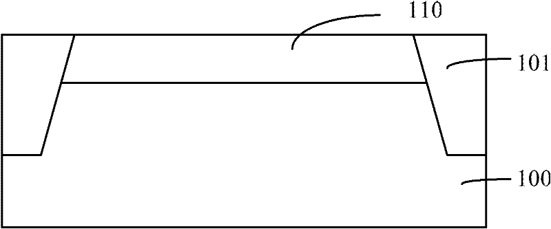
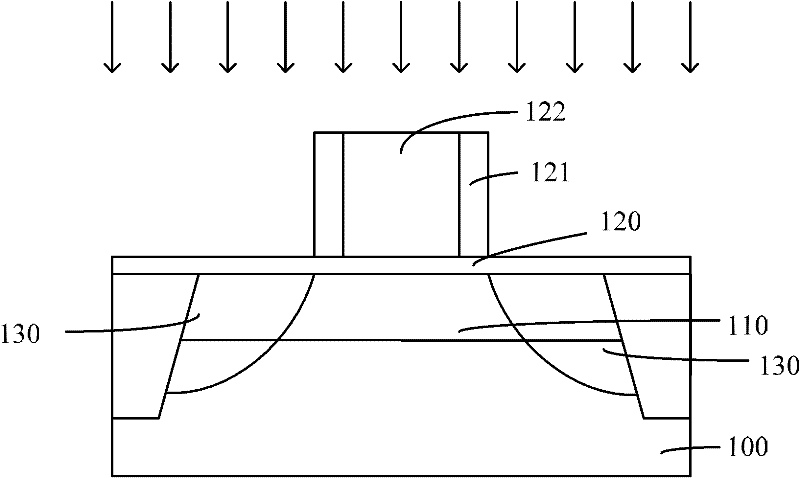
[0077] It can be seen from the background art that the carrier mobility of existing metal oxide semiconductor devices is relatively small. The inventors of the present invention investigated this and found that in the current semiconductor technology, metal oxide semiconductor devices are often fabricated on a semiconductor wafer having a single crystal orientation such as silicon. In particular, most of today's semiconductor devices are fabricated on the surface of silicon wafers with a (100) crystalline orientation. However, electrons have higher mobility in silicon wafers with (100) crystallographic orientation, while holes have higher mobility in silicon wafers with (110) crystallographic orientation. So (110) crystalline silicon wafers are most suitable for PMOS devices, but not for NMOS devices. In contrast, silicon wafers with a (100) crystalline orientation are most suitable for NMOS devices, but not for PMOS devices.

[0078] The inventor also found that stress can ...


PUM

PropertyMeasurementUnit
thicknessaaaaaaaaaa
thicknessaaaaaaaaaa
thicknessaaaaaaaaaa

Abstract

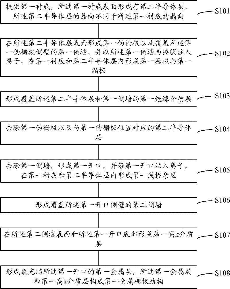
The invention relates to a metal oxide semiconductor structure and a forming method thereof, in particular to the forming method of a complementary metal oxide semiconductor device. The forming method disclosed by the invention has the advantages that, (1) the performances of the semiconductor device are improved by forming a semiconductor layer which has different crystal orientation with a substrate on the surface of the substrate and improving carrier mobility by utilizing stress generated in the semiconductor layer with the different crystal orientation; (2) the carrier mobility is improved by forming the semiconductor layer which has the different crystal orientation with the substrate on the surface of the substrate, forming an NMOS (negative-channel metal oxide semiconductor) on the crystal surface of orientation (100) and forming a PMOS (positive-channel metal oxide semiconductor) on the crystal surface of orientation (110); (3) the leakage current problem in the conventional process is avoided by substituting a high-k gate dielectric for a traditional silicon dioxide gate dielectric; and (4) the forming method has simple process and low cost.

Description

technical field [0001] The invention relates to a high-performance semiconductor device and its forming method, in particular to a metal oxide semiconductor device and its forming method. Background technique [0002] A metal-oxide-semiconductor (MOS) device and method of forming the same is disclosed in Chinese patent application publication No. CN1414617A, comprising: providing a substrate to accommodate a conductive device of a first conductivity type having a first device active region region; forming a gate electrode structure on the active region of the first device, the gate electrode structure including a gate electrode and an insulating sidewall; doping the exposed portion of the conductive region with the active region of the first device region has ions of the opposite conductivity type to form source and drain regions on opposite sides of the gate electrode structure; by selective chemical vapor deposition on the source and drain regions and on the gate A silici...

Claims


Application Information

Patent Timeline
Patent Type & Authority Applications(China)
IPC IPC(8): H01L29/78H01L29/04H01L29/51H01L21/336H01L21/28H01L21/265
Inventor 三重野文健
Owner SEMICONDUCTOR MANUFACTURING INTERNATIONAL (BEIJING) CORP
Why Eureka
Try Eureka