Quick-response photo-thermal induced voltage thin-film material and application

A technology of induced voltage and thin film materials, applied in the fields of light and heat induced voltage materials and devices

Inactive Publication Date: 2012-07-04
KUNMING UNIV OF SCI & TECH
View PDF2 Cites 10 Cited by
  • Summary
  • Abstract
  • Description
  • Claims
  • Application Information

AI Technical Summary

Problems solved by technology

In the thin film material system of perovskite structure and quasi-perovskite structure, the response time (re...

Method used


Image

  • Quick-response photo-thermal induced voltage thin-film material and application
  • Quick-response photo-thermal induced voltage thin-film material and application

Examples


Embodiment 1

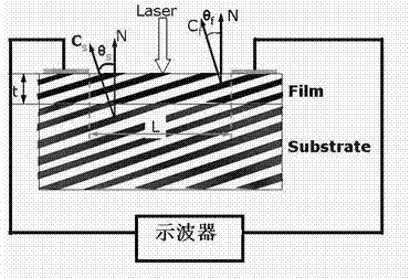
[0022] exist figure 1 Choose from La 1-x Sr x CoO 3 , where X=0.3 is a thin film material with fast response to laser-induced voltage effect. First, using pulsed laser deposition technology at an inclination angle of 10 o SrTiO 3 La grown on a single crystal substrate 1-x Sr x CoO 3 film; then follow the figure 1 Connect a high-frequency oscilloscope; irradiate the surface of the film with light, and then generate a light-induced voltage in the direction of the tilt angle, so that the induced voltage signal can be obtained and a corresponding image can be formed.

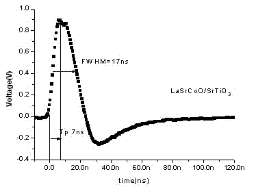
[0023] figure 2 In order to use the above method at an inclination angle of 10 o SrTiO 3 La grown on a single crystal substrate 0.5 Sr 0.5 CoO 3 Film, photo-induced voltage image obtained under 28ns pulse width UV laser (248nm) irradiation. It can be concluded that La 0.5 Sr 0.5 CoO 3 The response time of the film is 7ns, and the full width at half maximum is 17ns.

Embodiment 2

[0025] exist figure 1 Choose from La 1-x Sr x CoO 3 , where X=0.1 is used as a thin film material with fast response to laser-induced voltage effect. First, using pulsed laser deposition technology at a tilt angle of 15 o SrTiO 3 La grown on a single crystal substrate 1-x Sr x CoO 3 film; then follow the figure 1 Connect a high-frequency oscilloscope; irradiate the surface of the film with light, and then generate a light-induced voltage in the direction of the tilt angle, so that the induced voltage signal can be obtained and a corresponding image can be formed.

[0026] The photo-induced voltage image obtained under the irradiation of ultraviolet laser (248nm) with pulse width of 28ns. It can be concluded that La 0.5 Sr 0.5 CoO 3 The response time of the film is 7ns, and the full width at half maximum is 17ns.

Embodiment 3

[0028] exist figure 1 Choose from La 1-x Sr x CoO 3 , where X=0.6 is a thin film material with fast response to laser-induced voltage effect. First, using pulsed laser deposition technology at a tilt angle of 5 o SrTiO 3 La grown on a single crystal substrate 1-x Sr x CoO 3 film; then follow the figure 1 Connect a high-frequency oscilloscope; irradiate the surface of the film with light, and then generate a light-induced voltage in the direction of the tilt angle, so that the induced voltage signal can be obtained and a corresponding image can be formed.

[0029] The photo-induced voltage image obtained under the irradiation of ultraviolet laser (248nm) with pulse width of 28ns. It can be concluded that La 0.5 Sr 0.5 CoO 3 The response time of the film is 7ns, and the full width at half maximum is 17ns.


PUM


Abstract

The invention discloses a photo-thermal induced voltage thin-film material having response time of less than 10 ns, and the application of the material. Lal-xSrxCoO3 serves as a quick-response induced voltage material, wherein x is equal to 0.1 to 0.6. A thin film is grown on an inclined strontium titanate (SrTiO3) single-crystal substrate by using a pulse laser deposit technology and has photo-thermal radiation induced voltage effects. Pulse laser light of which the pulse width is 28 ns and the wavelength is 248 nm is irradiated to the thin film, a quick-response large voltage signal of which the response time is 7 ns and the full width at half maximum is 17ns is obtained in the inclination direction of the thin film, and the voltage signal is acquired by a high-frequency oscilloscope. The photo-thermal induced voltage thin-film material is characterized in that: the response time is short; the material can operate at a wide optical spectrum of 0.19 to 11 mu m; the operation flow is easy, and energy sources are saved; the material can be used for manufacturing quick-response photo-thermal induced voltage detector devices; the response speed of a photo-thermal measuring instrument is increased; and the material is applicable to sensitive detection and tracking of pulse photo-thermal signals and military targets in the technical field of industry and the field of life.

Description

technical field [0001] The invention relates to a fast-response induced voltage material and its application, and belongs to the technical field of light and heat induced voltage materials and devices. Background technique [0002] At present, light and heat measuring instruments are mainly divided into two categories: photon measuring instruments and calorimetric measuring instruments. Photon-type measuring instruments are based on the excitation of carriers by incident light in semiconductor materials, such as the generation of electron holes, to measure the energy of incident light. Such detectors usually have fast time response, but limited by energy bands and energy levels, they cannot work in a wide spectral range. The calorimetric measuring instrument will change the physical quantity when absorbing heat, and measure the light radiation by monitoring the physical quantity parameters. Such devices can work in a wide spectral range but take a long time to reach therma...

Claims


Application Information

Patent Timeline
IPC IPC(8): H01L35/22H01L35/28G01J1/42
Inventor 虞澜张鹏翔哈勃迈尔.汉斯.乌利希晏国文王勇
Owner KUNMING UNIV OF SCI & TECH
Why Eureka
Try Eureka