

Large area deposition of graphene hetero-epitaxial growth, and products including the same
一种异质外延、石墨烯的技术,应用在石墨烯、晶体生长、单晶生长等方向,能够解决降低电子特性等级、材料添加物污染等问题
- Summary
- Abstract
- Description
- Claims
- Application Information
AI Technical Summary
Problems solved by technology
Method used
Image

Examples
Embodiment Construction
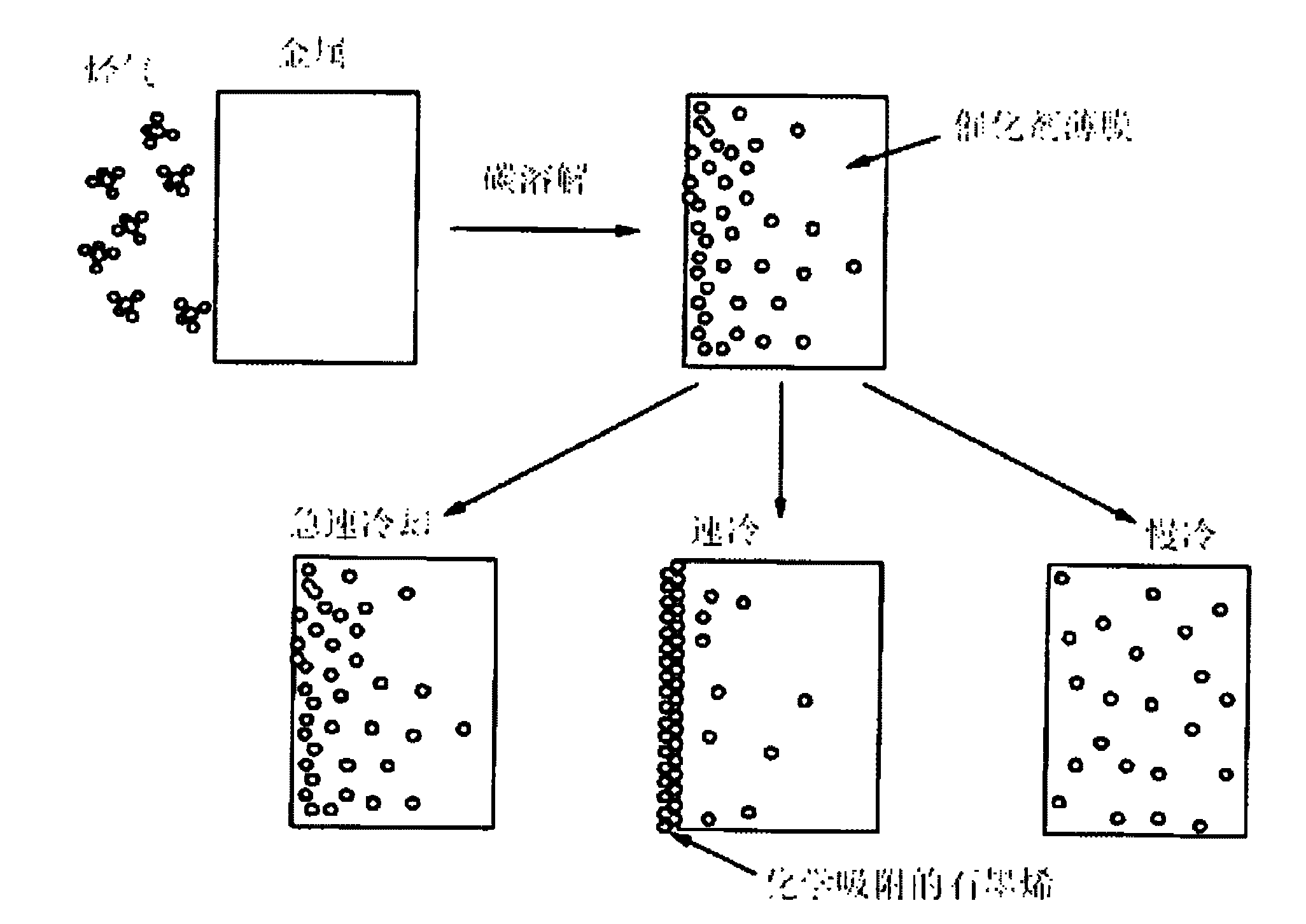
[0031] Certain exemplary embodiments of the present invention relate to heteroepitaxially grown single crystal graphite (n about 15) and extended techniques for its conversion to high electron grade (HEG) graphene (n<about 3). Certain example embodiments also relate to the use of HEG graphene in transparent (in the visible and infrared spectral range), ultra-thin conductive graphene films, e.g., for more general applicability for various applications including, e.g., solid-state solar cells Alternatives to metal oxide window electrodes. The growth technique illustrated by certain embodiments is based on a catalytically driven heteroepitaxial CVD process that generates temperatures low enough to be non-destructive to the glass. For example, according to the principles of thermodynamics and kinetics, HEG graphene films can be crystallized from the gas phase in a seed catalyst layer at a temperature of, for example, lower than about 600°C.
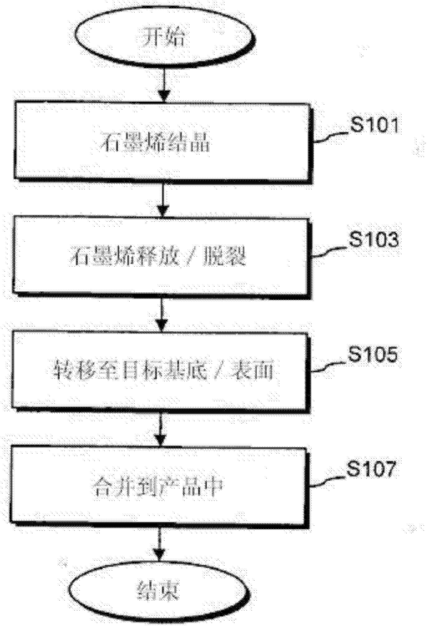
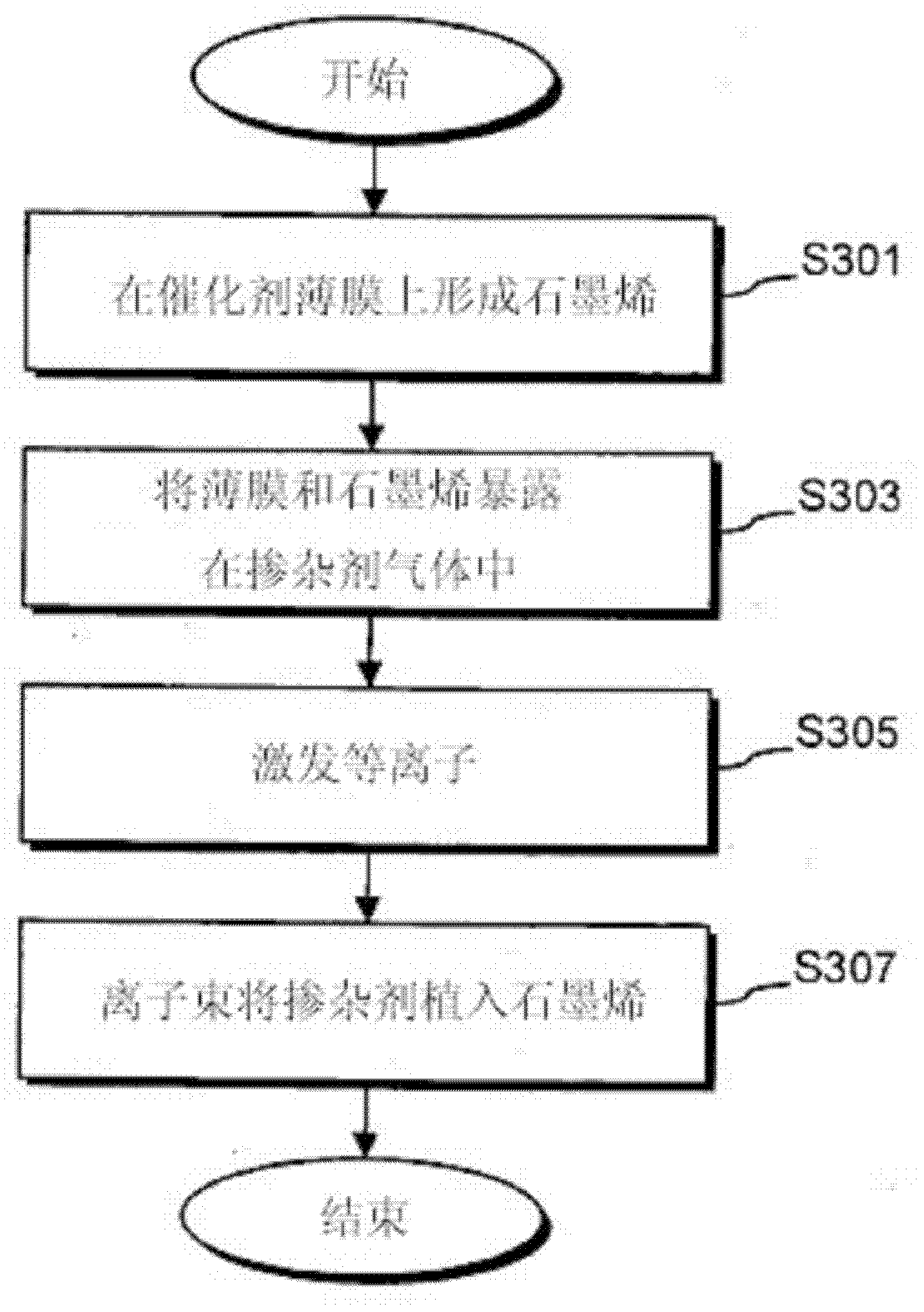
[0032] figure 1 A high-level flowcha...
PUM
| Property | Measurement | Unit |
|---|---|---|
| sheet resistance | aaaaa | aaaaa |
| electrical conductivity | aaaaa | aaaaa |
| transparency | aaaaa | aaaaa |
Abstract
Description
Claims
Application Information