

N-type casting monocrystalline silicon with uniform doping resistivity and preparation method thereof
A silicon single crystal, resistivity technology, applied in the field of solar cell materials, can solve the problems of low utilization rate of high-efficiency solar cell materials, large axial variation range of resistivity of N-type phosphorus-doped single crystal silicon ingots, etc. The effect of large-scale application, improved utilization, and simple operation
- Summary
- Abstract
- Description
- Claims
- Application Information
AI Technical Summary
Problems solved by technology
Method used
Image

Examples
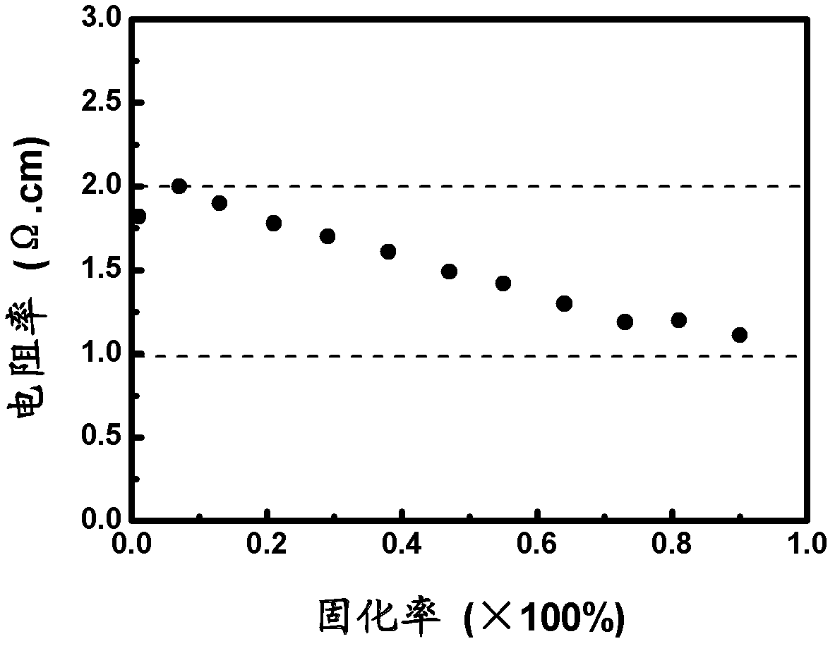
Embodiment 1
[0026] First, dislocation-free raw material single crystal silicon block with a thickness of 15mm was spread over the bottom of the crucible, and then 240kg of high-purity electronic polysilicon material was put into the crucible, and 53.04mg of phosphorus and 1.74g of gallium were mixed into the furnace. After vacuuming the furnace chamber, let in argon gas, adjust the position of the heat preservation cover in the furnace and heat it to 1440℃, so that the polysilicon material, phosphorous, gallium and the 5mm thick raw monocrystalline silicon block near the polysilicon are heated, and the temperature is maintained at 1440℃ Above, the 5mm thick raw material single crystal silicon block, phosphorous, gallium, and all polysilicon materials close to the polysilicon are melted into a liquid to form a silicon melt. Pass cooling air into the bottom of the crucible, and raise the insulation cover at a speed of 1mm / min, so that the silicon melt gradually solidifies from the bottom to t...
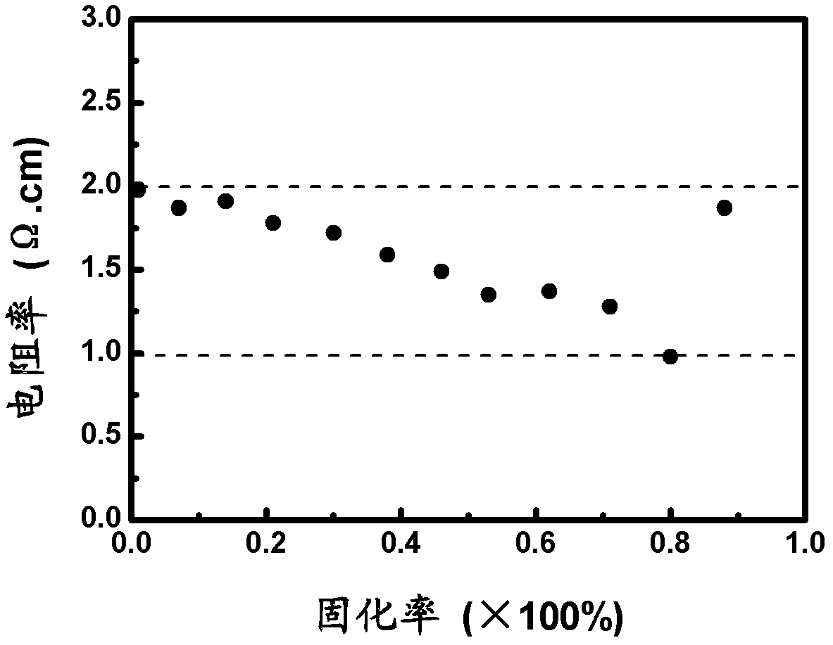
Embodiment 2
[0028] First, the dislocation-free raw material single crystal silicon block with a thickness of 20mm is spread all over the bottom of the crucible, and then 240kg of metallurgical grade boron-phosphorus-compensated polysilicon material (contains a total of 2.35mg of boron and 30.29mg of phosphorus) is put into the crucible and mixed at the same time. Put 45.46mg of phosphorus and 2.49g of gallium into the furnace. After vacuuming the furnace chamber, let in argon gas, adjust the position of the heat preservation cover in the furnace and heat it to 1450℃, so that the polysilicon material, phosphorus, gallium and the 7mm thick raw monocrystalline silicon block close to the polysilicon are heated, and the temperature is maintained at 1450℃ Above, the 7mm thick raw material single crystal silicon block, phosphorous, gallium, and all polysilicon materials close to the polysilicon are melted into liquid to form a silicon melt. Pass cooling air into the bottom of the crucible, and ra...
PUM
 Abstract
Description
Claims
Application Information