NAND flash memory controller supporting operation out-of-order execution

A memory controller and flash memory control technology, which is applied in the direction of instruments, electrical digital data processing, etc., can solve the problem of limited number of memory access operations

Active Publication Date: 2012-07-11
NAT UNIV OF DEFENSE TECH
View PDF3 Cites 9 Cited by
  • Summary
  • Abstract
  • Description
  • Claims
  • Application Information

AI Technical Summary

Problems solved by technology

In the sequential structure, only a single substrate can be busy at a certain moment, and at most can only use the memory access performance of a single-substrate memory chip

Method used


Image

  • NAND flash memory controller supporting operation out-of-order execution
  • NAND flash memory controller supporting operation out-of-order execution
  • NAND flash memory controller supporting operation out-of-order execution

Examples


Embodiment Construction

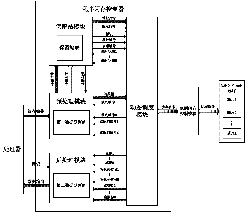
[0050] figure 1 Is the overall structure block diagram of the present invention.

[0051] The present invention is placed between the processor CPU and the low-level flash memory control module, the low-level flash memory control module is connected with the chip, the chip is a NAND Flash chip, and contains M substrates inside, and M is a positive integer power of 2, generally 4. The invention is composed of a preprocessing module, a reservation station module, a dynamic scheduling module and a postprocessing module. The low-level flash memory control module connected with the present invention is formed by parallel connection of M sequential memory controllers mentioned in the background art, and respectively controls M substrates in the chip.

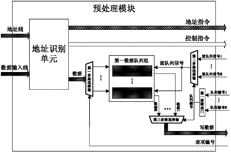
[0052] The preprocessing module is connected with the processor, the reservation station module, and the dynamic scheduling module, and contains the first data queue group. The preprocessing module receives control instructions and a...


PUM


Abstract

The invention discloses a NAND flash memory controller supporting operation out-of-order execution, and aims to improve memory access data throughput. The controller consists of a preprocessing module, a reservation station module, a dynamic scheduling module and a postprocessing module, wherein the preprocessing module consists of an address recognition unit, three multiplexers, a first data queue group and a first logic OR gate; the reservation station module consists of two multiplexers, a table entry number register, a validity monitoring unit, a relevance judgment unit, a substrate state setting unit, an output judgment unit, a control logic unit and a reservation station table; the dynamic scheduling module consists of five multiplexers, M state machines, an arbiter and a second logic OR gate; and the postprocessing module consists of a comparator, a second data queue group and a multiplexer. By the controller, the memory access operation of different substrates of a memory chip can be subjected to parallel execution, the working parallelism of the substrates is improved, and the memory access data throughput is effectively improved.

Description

technical field [0001] The invention relates to a storage controller of NAND flash (ie, NAND Flash) storage chip particles, in particular to a storage controller supporting out-of-order execution of operations. Background technique [0002] With the continuous development of integrated circuit technology, the volume of NAND Flash storage chip particles decreases by 40% to 50% every year, while the capacity of chip particles doubles every year. At the same time, the advancement of NAND Flash integrated circuit technology has gradually developed the internal organization structure of chip particles from traditional monomer and single substrate to multi-body and multi-substrate. For example, Micron's MT29H32G08GCAH2 memory chip has a capacity of 32Gb and contains four substrates inside. The four substrates share the I / O bus and five control signal lines: address latch signal (ALE), command latch signal (CLE), write enable signal (WE#), read enable signal (RE# ) and write-prot...

Claims


Application Information

Patent Timeline
IPC IPC(8): G06F13/16
Inventor 肖侬赖明澈黄立波陈博
Owner NAT UNIV OF DEFENSE TECH
Why Eureka
Try Eureka