
Solar cell structure with wide spectrum high absorption and manufacturing method thereof

A technology of solar cells and manufacturing methods, which is applied in the manufacture of circuits, electrical components, and final products, and can solve the problems of narrow absorption spectrum and low absorption rate, and achieve the effects of low cost, improved absorption, and simple process

Inactive Publication Date: 2012-07-11
INST OF SEMICONDUCTORS - CHINESE ACAD OF SCI
View PDF5 Cites 11 Cited by
  • Summary
  • Abstract
  • Description
  • Claims
  • Application Information

AI Technical Summary

Problems solved by technology

[0007] The purpose of the present invention is to provide a broad-spectrum high-absorption solar cell structure and its manufacturing method to solve the problems of narrow absorption spectrum and low absorption rate of traditional silicon cells, thereby improving the photoelectric conversion efficiency of silicon-based solar cells

Method used


Image

  • Solar cell structure with wide spectrum high absorption and manufacturing method thereof
  • Solar cell structure with wide spectrum high absorption and manufacturing method thereof
  • Solar cell structure with wide spectrum high absorption and manufacturing method thereof

Examples


Embodiment Construction

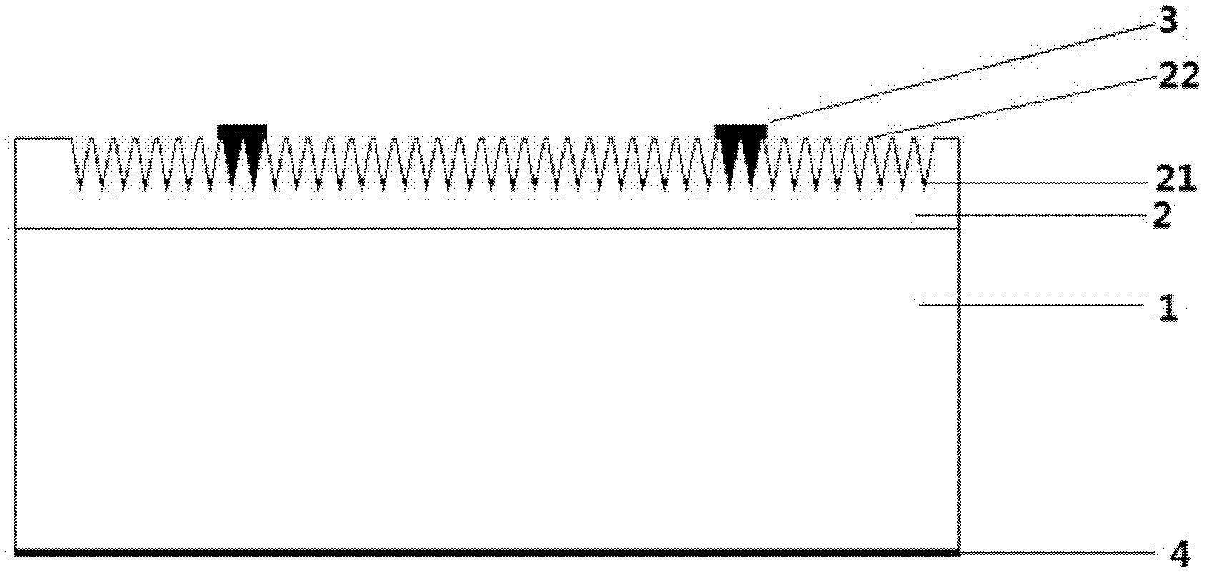
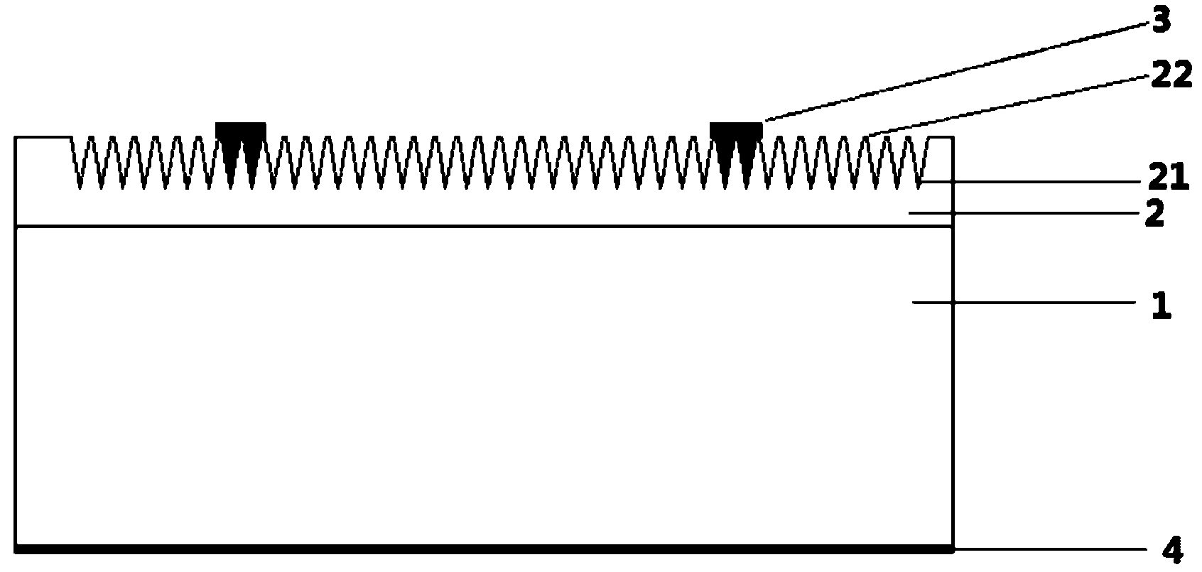
[0026] see figure 1 As shown, the present invention provides a broad-spectrum high-absorption solar cell structure, comprising:

[0027] A p-type or lightly doped n-type silicon layer 1, the silicon substrate has a (100) crystal orientation, its thickness is 200 to 600 μm, and its resistivity is 0.1 to 10 Ω·cm;

[0028] A chalcogenide-doped layer 2, the chalcogenide-doped layer 2 is silicon material doped with chalcogenides, the chalcogenide-doped layer 2 is fabricated on the p-type or lightly doped n-type silicon layer 1 , the doping concentration of the chalcogenide doped layer 2 is 10 17 to 10 20 cm -3 , the surface of the chalcogenide-doped layer 2 is fabricated with an array-like continuous cone structure 22, the height of the cone structure 22 is 0.1 μm to 10 μm, the diameter is 20 nm to 5 μm, and the distance between the apexes of each cone is 20nm to 5μm, the bottom of the gap between the pointed cone structures 22 is deposited silver nanoparticles 21, and the diam...


PUM

PropertyMeasurementUnit
Heightaaaaaaaaaa
Diameteraaaaaaaaaa
Diameteraaaaaaaaaa

Abstract

The invention provides a solar cell structure with wide spectrum high absorption. The structure comprises: a p type or lightly doped n type silicon layer; a sulfur system element doping layer which is silicon material doped with sulfur system elements, wherein the sulfur system element doping layer is manufactured on the p type or lightly doped n type silicon layer, a surface of the sulfur system element doping layer is provided with sharp cone structures in array succession, and a gap bottom between the sharp cone structures has deposited silver nano particles; a plurality of upper surface contact gate electrodes which are manufactured on surfaces of the sharp cone structures; and a lower electrode which is manufactured at a back side of the p type or lightly doped n type silicon layer. According to the structure and the method of the invention, light absorption and photoelectric conversion efficiency can be raised. Simultaneously, the structure and the method have the characteristics of simple technology, low cost and the like. Simultaneously, the silver nano particles which play a catalysis role in technology also can be utilized to generate a surface plasma wave effect to attain two objectives by a single move.

Description

technical field [0001] The invention relates to the field of silicon-based solar cells, in particular to a broad-spectrum high-absorption solar cell structure and a manufacturing method thereof. Background technique [0002] With the development of the global economy, the consumption of energy has increased dramatically. Currently, the vast majority of energy is obtained by burning fossil fuels. The large amount of carbon dioxide and other gas emissions caused by the energy use of fossil fuels is causing increasingly serious social and environmental problems. Therefore, the development and utilization of various renewable energy sources has received more and more attention from the international community. Among all kinds of renewable energy, solar energy has become the focus of development because of its inexhaustible, inexhaustible, pollution-free, and convenient features. The utilization of solar energy mainly includes two categories: solar thermal and photovoltaic. Am...

Claims


Application Information

Patent Timeline
IPC IPC(8): H01L31/0352H01L31/0288H01L31/18
CPCY02P70/50
Inventor 刘孔曲胜春谭付瑞唐爱伟金兰张君梦徐文清
Owner INST OF SEMICONDUCTORS - CHINESE ACAD OF SCI
Learn More