Supercharge Your Innovation With Domain-Expert AI Agents!

Flexible semiconductor device and manufacturing method therefor

A manufacturing method and semiconductor technology, applied in the fields of semiconductor/solid-state device manufacturing, semiconductor devices, organic semiconductor devices, etc., can solve problems such as hindering high-speed operation, and achieve reduction of parasitic capacitance and leakage current, high-performance productivity, and improvement of Effects of Features

Active Publication Date: 2012-07-11
PANASONIC INTPROP MANAGEMENT CO LTD
View PDF6 Cites 3 Cited by
  • Summary
  • Abstract
  • Description
  • Claims
  • Application Information

AI Technical Summary

Problems solved by technology

[0015] However, miniaturization, high integration, and multilayering of the TFT element used in the display section or the drive section of the display device, and the elements and wiring of peripheral circuits are required. When the drain electrode and the gate electrode are sequentially formed on the substrate and multilayered to form a TFT element, if the wiring is multilayered, parasitic capacitance will be generated between the wiring arranged up and down through the interlayer insulating film , Sometimes there is a problem that hinders the speed-up of the operation

Method used


Image

  • Flexible semiconductor device and manufacturing method therefor
  • Flexible semiconductor device and manufacturing method therefor
  • Flexible semiconductor device and manufacturing method therefor

Examples


Embodiment approach 1

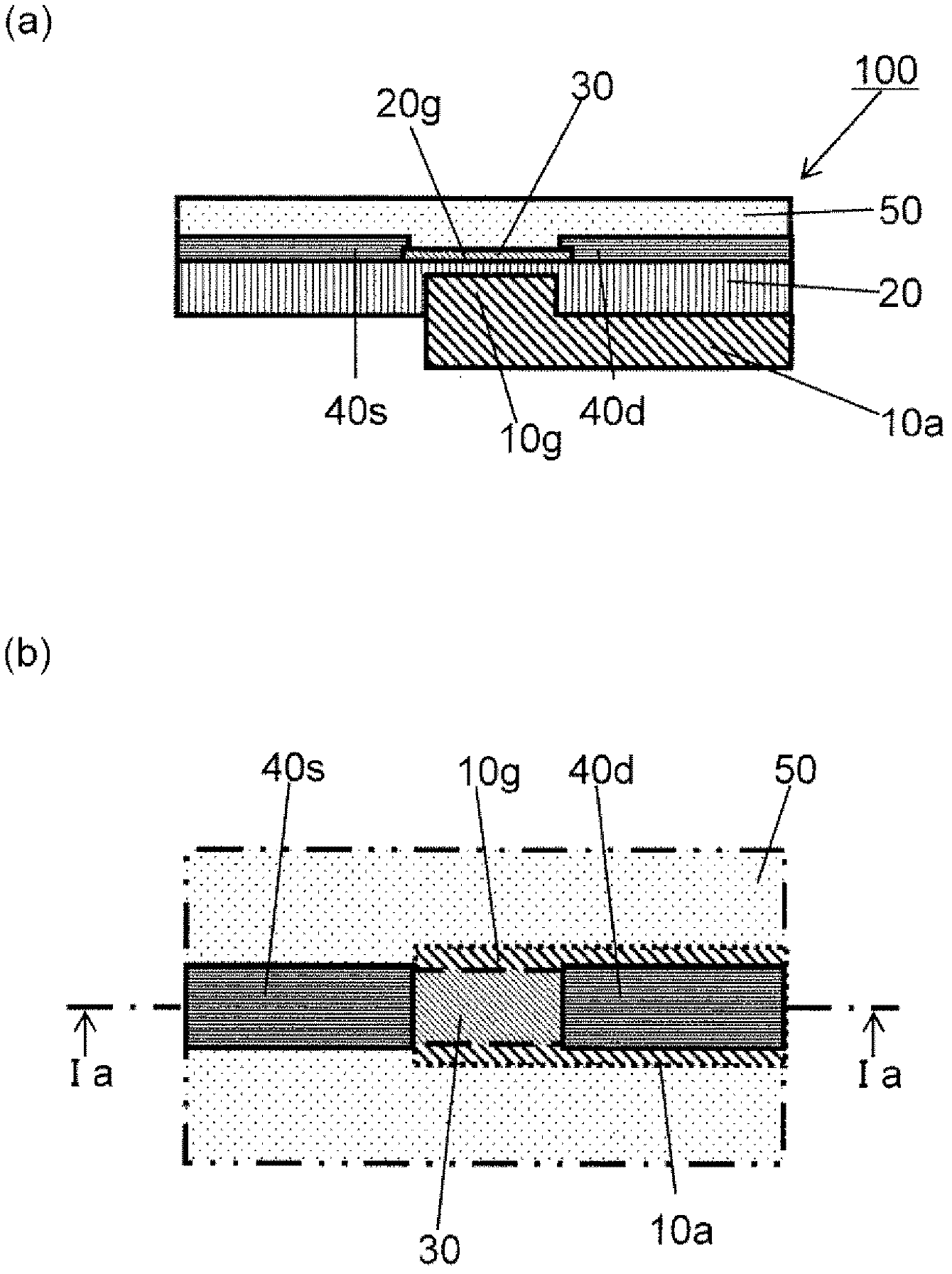
[0075] refer to figure 1 (a) and (b) describe the flexible semiconductor device 100 according to Embodiment 1 of the present invention.

[0076] figure 1 (b) is a schematic diagram of the upper surface of the flexible semiconductor device 100, figure 1 (a) to represent figure 1 (b) Schematic cross-sectional view of the Ia-Ia section.

[0077] The flexible semiconductor device 100 includes the following parts: an insulating film 20; a source electrode 40s and a drain electrode 40d formed on the insulating film 20; a semiconductor layer 30; and the insulating film 20 also functions as a gate insulating film. A gate insulating film 20g, a TFT structure composed of a gate electrode 10g, and a lower wiring pattern layer 10a drawn out from the gate electrode 10g and functioning as a wiring portion.

[0078] The sealing layer 50 also functions as a base material supporting the TFT structure, and is preferably made of a flexible resin material that is bendable even after curing. ...

Embodiment approach 2

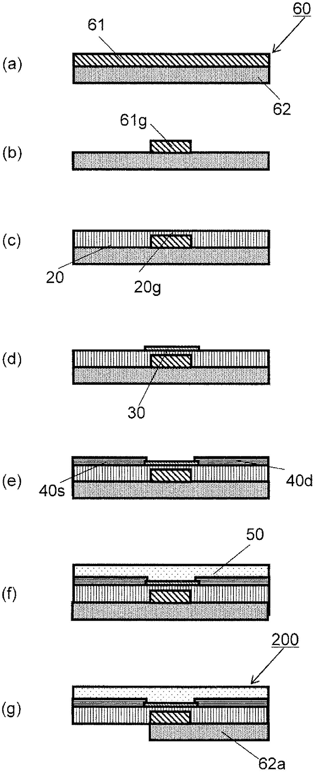
[0108] image 3 The structure of the flexible semiconductor device 200 related to one embodiment of the present invention is shown. In this second embodiment, the point of difference from the above-mentioned first embodiment is that a multilayer metal foil having a structure of two or more layers of different metal materials is used. That is, the prepared metal foil has a multilayer structure, and the gate electrode 10g and the lower wiring pattern layer 10a are formed of different metal materials.

[0109] refer to image 3 (a)-(g) demonstrate an example of the manufacturing process of this Embodiment 2. In addition, description of portions overlapping with Embodiment 1 will be omitted except for matters particularly mentioned.

[0110] First, if image 3 As shown in (a), the multilayer metal foil 60 in which the first metal layer 61 and the second metal layer 62 are sequentially laminated is prepared. The metal constituting the first metal layer 61 and the second metal ...

Embodiment approach 3

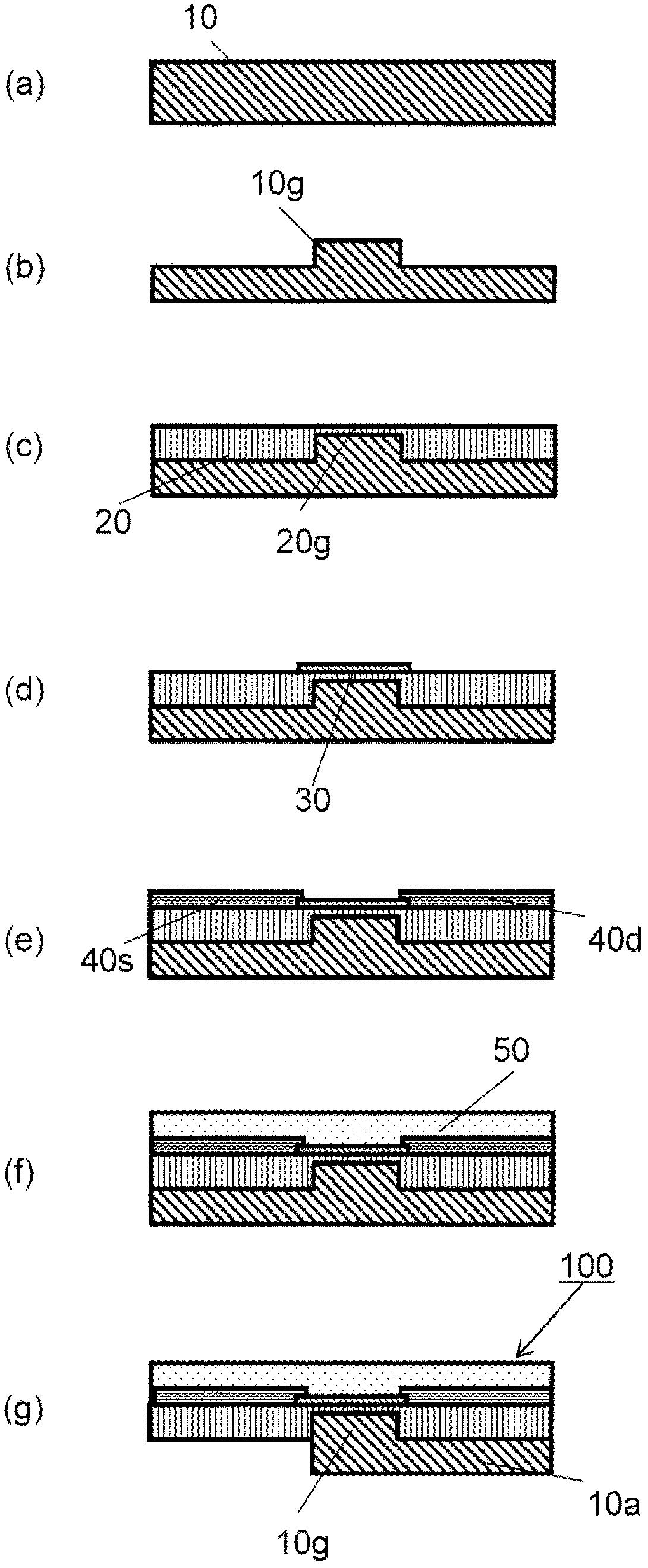
[0116] Figure 4 The configuration of a flexible semiconductor device 300 according to an embodiment of the present invention is shown. This third embodiment differs from the first embodiment described above in that the second insulating film 21 is formed together with the insulating film 20 in the concave portion formed in the metal foil 10 . refer to Figure 4 (a)-(h) An example of this manufacturing process is demonstrated. In addition, description of portions overlapping with Embodiment 1 will be omitted except for matters particularly mentioned.

[0117] First, if Figure 4 As shown in (a), the metal foil 10 is prepared (produced, purchased, etc.). In this embodiment, the metal foil 10 can use the SUS foil of thickness 70 micrometers, for example.

[0118] Next, if Figure 4 As shown in (b), by etching the metal foil 10 , protrusions serving as gate electrodes or capacitor electrodes and other recesses are formed on the surface of the metal foil 10 .

[0119] Next,...


PUM


Abstract

Disclosed are a flexible semiconductor device and manufacturing method therefor whereby the capacitances of capacitor parts of semiconductor elements and the like can be increased while decreasing parasitic capacitances that arise between multilevel interconnections. The disclosed flexible semiconductor device is provided with an insulating film on which a semiconductor element is formed. The top and bottom surfaces of the insulating film have a top wiring pattern layer and a bottom wiring pattern layer, respectively. The semiconductor element comprises: a semiconductor layer formed on the top surface of the insulating film; a source electrode and a drain electrode formed on the top surface of the insulating film so as to contact the semiconductor layer; and a gate electrode formed on the bottom surface of the insulating film so as to be opposite the semiconductor layer. A first thickness, which is the thickness of the insulting film facing the source electrode, the drain electrode, the top wiring pattern layer, and the bottom wiring pattern layer, is greater than a second thickness, which is the thickness of the insulating film between the gate electrode and the semiconductor layer.

Description

technical field [0001] The present invention relates to a flexible semiconductor device and a manufacturing method thereof. Background technique [0002] With the spread of information terminals, demand for flat panel displays as displays for computers is increasing. In addition, with the further development of informatization, the information provided by paper media in the past has more opportunities to be digitized. As a thin, light, mobile office display medium that can be easily moved, the demand for electronic paper or digital paper is also increasing. It is improving (Patent Document 1, etc.). [0003] Generally, in a flat panel display, an element utilizing liquid crystal, organic EL (organic electroluminescence), electrophoresis, or the like is used to form a display medium. In addition, in order to ensure the uniformity of screen luminance, screen update speed, and the like in such display media, technologies employing active drive elements (TFT elements) as image...

Claims


Application Information

Patent Timeline
Patent Type & Authority Applications(China)
IPC IPC(8): H01L21/336H01L21/28H01L21/822H01L21/8234H01L27/04H01L27/06H01L29/423H01L29/49H01L29/786H01L51/50H05B33/02H05B44/00
CPCH01L2251/5338H01L29/78603H01L27/1292H01L27/3244H01L27/1225H01L27/1262H01L29/7869H01L27/124H10K59/12H10K2102/311
Inventor 一柳贵志中谷诚一平野浩一
Owner PANASONIC INTPROP MANAGEMENT CO LTD
Features
  • R&D
  • Intellectual Property
  • Life Sciences
  • Materials
  • Tech Scout
  • Unparalleled Data Quality
  • Higher Quality Content
  • 60% Fewer Hallucinations
Learn More