Hermetic package with getter materials
A technology of absorber and adhesive, which is applied in the field of packaging of organic light-emitting devices, and can solve the problems of reducing device efficiency, device light output and aesthetic appearance loss, etc.
- Summary
- Abstract
- Description
- Claims
- Application Information
AI Technical Summary
Problems solved by technology
Method used
Image
Examples
example 1
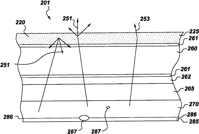
[0033] exist Image 6 In the illustrated embodiment, device 600 is built on substrate 660 . Device 600 includes a first electrode (anode) 665 , a light emitting layer 670 and a top electrode (cathode) 685 having a highly reflective surface 686 facing substrate 660 .
[0034] The OLED device is packaged in a hermetic package consisting of a rear membrane 630 and a transparent front membrane 606 . The front diaphragm 606 placed on the light emitting side 601 of the device 600 has a hard coat layer 607 and a water vapor barrier layer 610 on both sides. The two membranes 606 and 630 are bonded to each other along the peripheral region with a suitable encapsulant 635 and the OLED device 600 is centered.
[0035] The rear membrane 630 is machined from a multilayer material including a thin interface layer 635 of adhesive and an aluminum barrier layer. The rear membrane 630 was degassed at 100°C for 12 hours. Dry CaO absorbent 625 in powder form was spread on a first film 621 of ...
example 2
[0040] exist Figure 7 In the illustrated embodiment, the device 700 is built on a substrate 760 with a hard coating 761 on both sides. Device 700 includes a first electrode (anode) 765 , a light emitting layer 770 and a top electrode (cathode) 785 with a highly reflective surface 786 facing substrate 760 .
[0041] The OLED device is packaged in a hermetic package consisting of a rear membrane 730 and a transparent front membrane 706 . The front diaphragm 706 on the light emitting side 701 of the device 700 has a hard coat layer 707 and a moisture barrier layer 710 on both sides thereof. The two membranes 706 and 730 are bonded to each other along the peripheral region with a suitable sealant 735 .
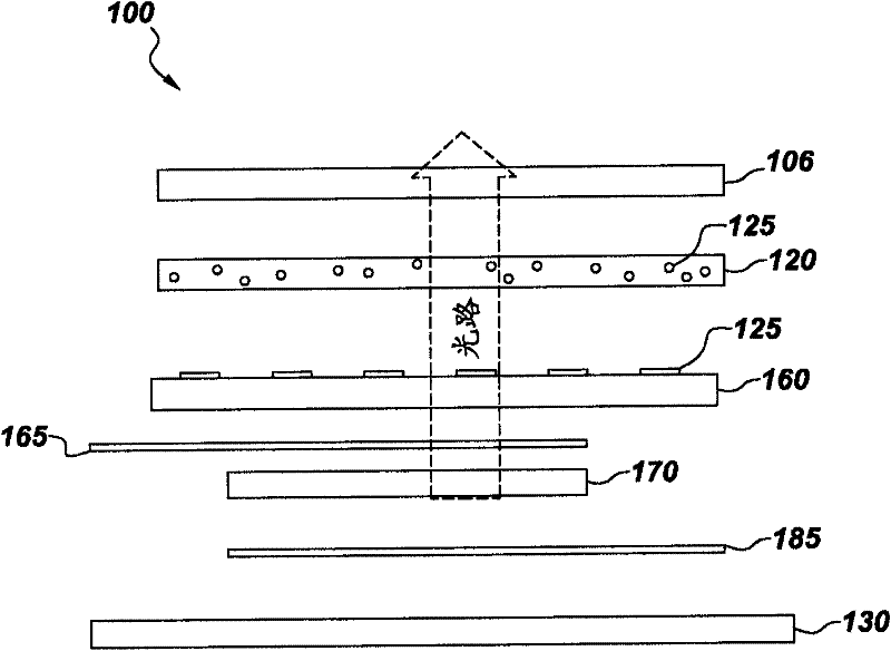
[0042]The absorber is deposited on the hard coat layer 761 of the transparent substrate 760 in a recurring pattern of dots 725 . Thus, the absorber is in the optical path on the light-emitting side 701 of the device 700 . The side of the absorber material facing the light fro...
PUM
| Property | Measurement | Unit |
|---|---|---|
| Particle size | aaaaa | aaaaa |
| Particle size | aaaaa | aaaaa |
Abstract
Description
Claims
Application Information
 - R&D Engineer
- R&D Manager
- IP Professional
- Industry Leading Data Capabilities
- Powerful AI technology
- Patent DNA Extraction
Browse by: Latest US Patents, China's latest patents, Technical Efficacy Thesaurus, Application Domain, Technology Topic, Popular Technical Reports.
© 2024 PatSnap. All rights reserved.Legal|Privacy policy|Modern Slavery Act Transparency Statement|Sitemap|About US| Contact US: help@patsnap.com


