Metal seal packaging for organic light emitting diode device

a technology of organic light-emitting diodes and seal packaging, which is applied in the direction of discharge tubes/lamp details, discharge tubes luminescnet screens, electric discharge lamps, etc., can solve the problems of oled's longevity, device useless as a display, and deterioration of oled performance, so as to enhance the life performance and suppress the permeation of moistur

Inactive Publication Date: 2007-04-10
ORGANIC LIGHTING TECH
View PDF4 Cites 64 Cited by
  • Summary
  • Abstract
  • Description
  • Claims
  • Application Information

AI Technical Summary

Benefits of technology

[0027]From the foregoing it is clear that a good hermetic seal is necessary to suppress the permeation of moisture and oxygen in to the OLED device to enhance the life performance of OLED. The best sealing material known to perform this function effectively is metal. The width of the seal needs to be in the substantial fractions of millimeter. This invention is on the perimeter metal sealing of OLED employing low melting eutectic alloys of solder metals. Illustration, shown subseque

Problems solved by technology

As a result, one of the major problems faced by OLED is its longevity.
The presence of oxygen and water vapor beyond one part per million (ppm) inside the device can deteriorate the performance of OLED.
Uniform degradation of light output, due to intrinsic aging nature of organic materials, can still render the device useful as a display with reduced brightness, whereas the black spots tend to spread, both during operation and storage, and thus render the device useless as a display.
Hence the latter mechanism is more serious than the first.
Width of the seal, for planar geometry like OLED, plays a major role due to the permeation length and hence dimensions of width in the range of microns is totally insufficient.
Before this reaction is complete, the moisture can pass through pin-holes to the sensitive layers of the device and damage the device.
Hence, this is not a reliable method.
Further, these films deposited through plasma enhanced chemical vapor d

Method used


Image

  • Metal seal packaging for organic light emitting diode device
  • Metal seal packaging for organic light emitting diode device
  • Metal seal packaging for organic light emitting diode device

Examples


Embodiment Construction

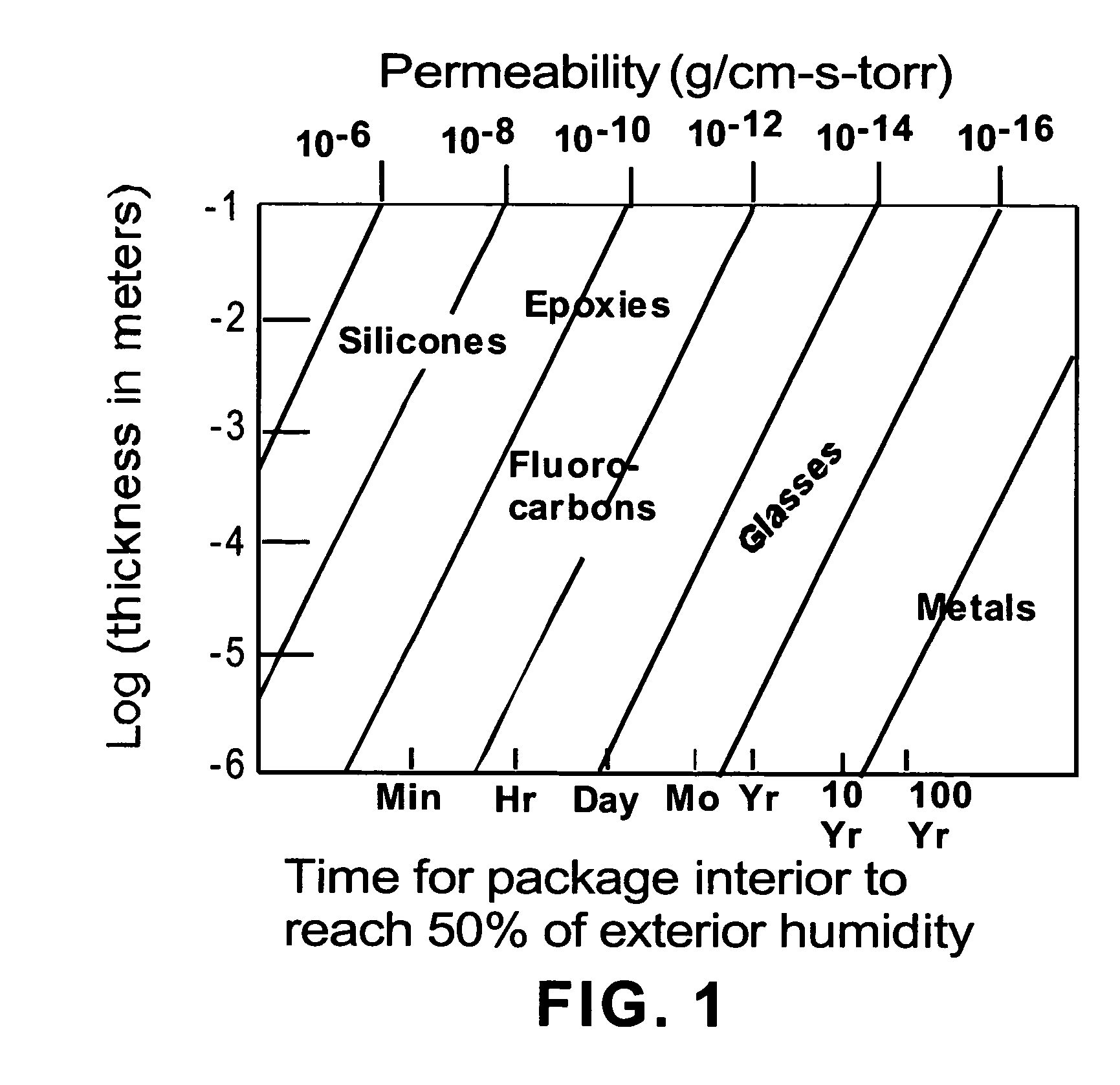
[0045]FIG. 1 is a graphic illustration of moisture permeation through different materials of seal with different thickness plotted on Y-Axis and the time for the interior of the device to reach 50% of the exterior humidity plotted at the bottom of X-Axis. At the top of X-Axis is plotted the permeability in gms / cm, sec, torr for various materials. FIG. 1 depicts the thickness of the sealant, through which moisture permeates, starting from 1 micron on Y-Axis. For a thickness of 1 micron, it is evident from FIG. 1 that for metal seal, it takes years for the interior of the device to reach 50% of exterior humidity. Under these conditions, epoxy seals take only days to reach 50% of exterior humidity. Although the devices like OLED will be terminating its life performance by the time the interior humidity reaches 50%, the graph illustrates that the metal seals are the best against moisture permeation.

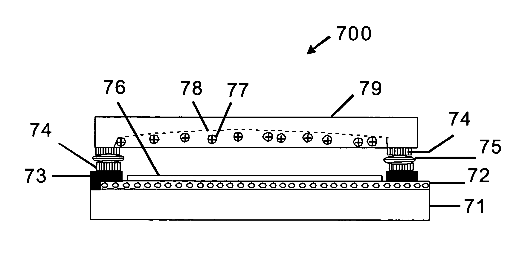
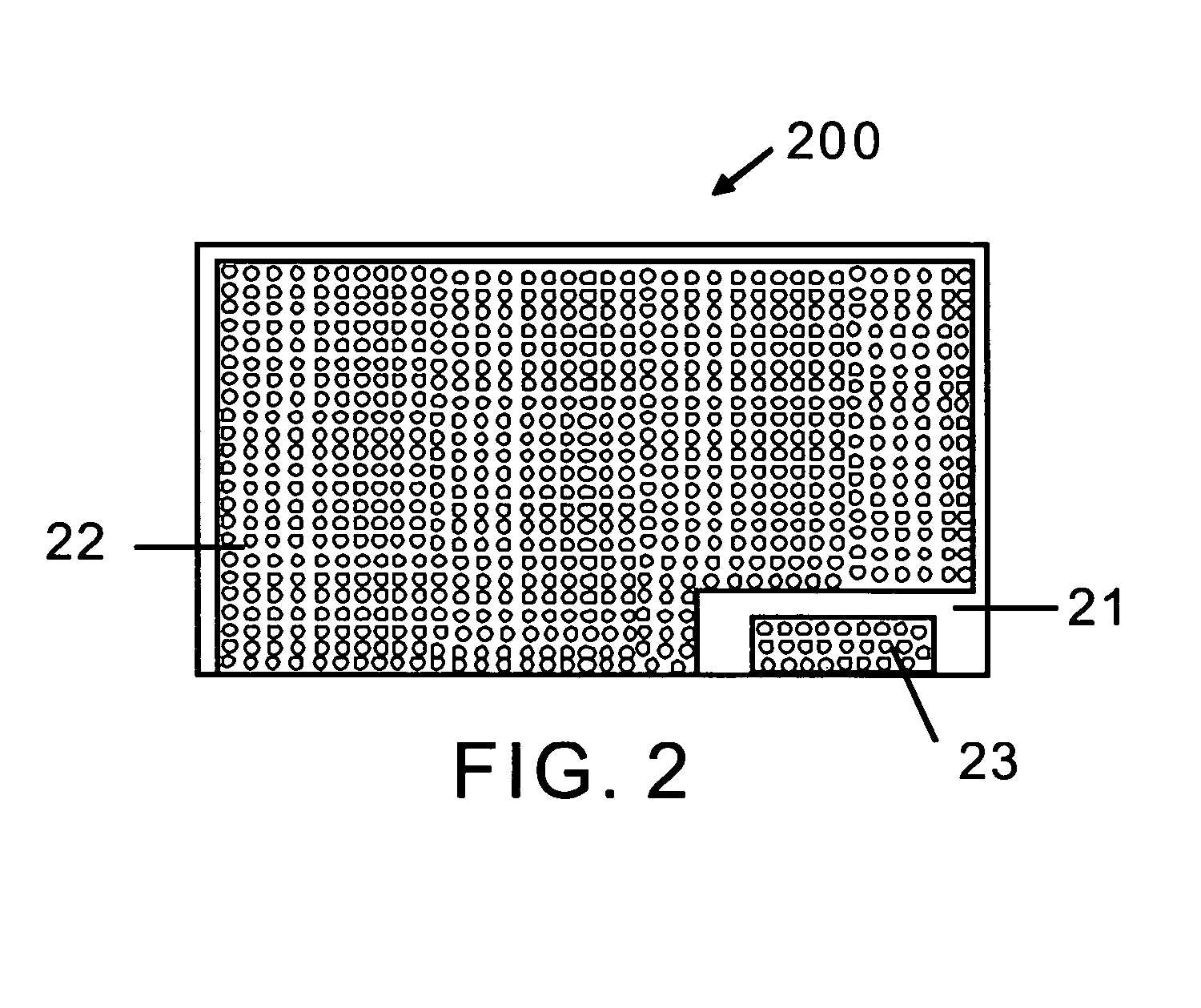
[0046]FIG. 2 is the bottom substrate 200 containing the transparent anode 22 of OLED and ...


PUM


Abstract

A metal sealed organic light emitting diode device comprising a lid, containing a recessed portion to accommodate large quantity of getter/dessicant, a band of metal stack at the perimeter over which is laid a band of low temperature melting solder alloy, pre-tinned subsequently, and a substrate. The substrate containing organic light emitting diode at the central area with a band of metal stack at the perimeter. The lid and the substrate are placed together in substantial alignment such that the pre-tinned low melting solder band of the lid contacts the metal stack of the substrate and thermally sealed in a controlled atmosphere. Multiples of substrates are sealed with a single lid containing multiplicity of recessed portions with multi-segmented metal stack and pre-tinned solder band to derive a large area device.

Description

CROSS REFERENCE TO RELATED APPLICATION[0001]Benefit of Provisional Application No. 60 / 461,099 filed Apr. 8, 2003[0002]U.S. Pat. No. 6,608,283—Liu et.al, Aug. 19, 2003.[0003]U.S. Pat. No. 6,198,220—Jones et.al, Mar. 6, 2001[0004]U.S. Pat. No. 6,706,316—Ghosh et.al, Mar. 16, 2004[0005]U.S. Pat. No. 6,570,325—Graff et.al, May 27, 2003[0006]U.S. Pat. No. 6,614,057—Silvernail et.al, Sep. 2, 2003OTHER PUBLICATIONS[0007]R. K. Traeger, “Hermeticity of ploymeric lid sealants”—Proceedings of 25th Electronics Components conference, pp. 361–367, April 1976[0008]Yoshihisa Tsuruoka et.al, “Transparent thin film dessicant for OLEDs”-pp. 860–863,[0009]Digest of Technical papers, SID′03, May 2003.[0010]D. C. Jones et.al, “Water ingression and condensation in sealed system”—Proceedings of Nat. Tech. Conf. On plastics in packaging, p. 45, 1969.[0011]W. J. Kass,—unpublished work, Sandia Labs / Albuquerque, N. Mex., May 1974STATEMENT REGARDING FEDERALLY SPONSORED RESEARCH OR DEVELOPMENT[0012]Not Applicabl...

Claims


Application Information

Patent Timeline
IPC IPC(8): H05B33/00F02FH01J1/62H01L21/56H01L51/52
CPCH01L51/5237H10K50/8423H10K50/846H10K50/8426
Inventor ANANDAN, MUNISAMY
Owner ORGANIC LIGHTING TECH
Why Eureka
Try Eureka