
Wax-free grinding and polishing template with double inlaying layers

A double inlay and inlay layer technology, which is applied in the direction of grinding tools, can solve the problems of high replacement cost, large thickness deviation of silicon wafers, wax pollution, etc., and achieve the effects of improving polishing efficiency, reducing thickness deviation, and reducing production costs

Active Publication Date: 2012-07-18
天津西美半导体材料有限公司 +1
View PDF9 Cites 8 Cited by
  • Summary
  • Abstract
  • Description
  • Claims
  • Application Information

AI Technical Summary

Problems solved by technology

[0002] In the processing of semiconductor materials, silicon wafers, sapphire and gallium arsenide, as the basic materials of common semiconductor devices and integrated circuits, often need to be polished, and the quality of the polishing technology will directly affect the quality of silicon wafers, sapphire and gallium arsenide. The surface quality of gallium arsenide and the performance of semiconductor devices. There are two main traditional polishing techniques: wax polishing and wax-free polishing. The wax technique is to bond and fix silicon wafers, sapphire or gallium arsenide to ceramic discs. On the flat plate, the polishing head drives the ceramic disc to rotate on the polishing cloth during polishing, and the polishing purpose is achieved under the action of mechanical pressure and polishing liquid. Practice has found that this kind of wax polishing has the defects of wax pollution and low polishing accuracy. With the electronic With the rapid development of technology and the increasing integration of large-scale integrated circuits, people's requirements for semiconductor devices are becoming more and more stringent, so the advantages of wax-free polishing are gradually reflected. The existing wax-free polishing technology, Chinese patent CN87202507 Relate to a kind of wax-free polishing pad, find in long-term use process: this kind of wax-free polishing pad has following defect: one, because this kind of wax-free polishing pad is a single mosaic layer, so its polishing efficiency is low, can't satisfy The demand of large-scale industrial production; 2. The adsorption layer of the polishing pad is extremely prone to wear and tear. When the adsorption layer wears out, the entire polishing pad must be replaced, so the replacement cost is relatively high; 3. The thickness deviation (TTV) of the silicon wafer after polishing is relatively high. Large, unable to meet high standard technical requirements

Method used


Image

  • Wax-free grinding and polishing template with double inlaying layers
  • Wax-free grinding and polishing template with double inlaying layers
  • Wax-free grinding and polishing template with double inlaying layers

Examples


Embodiment Construction

[0022] In order to further understand the content, characteristics and effects of the present invention, the following examples are given, and detailed descriptions are as follows in conjunction with the accompanying drawings:

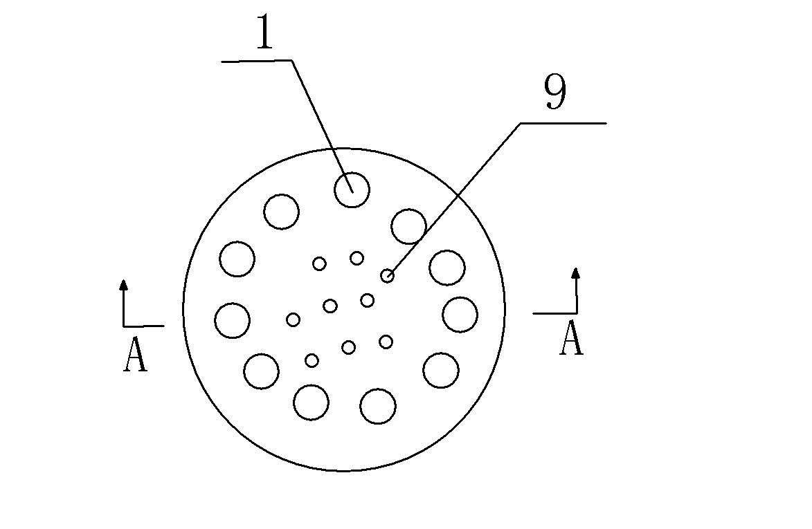
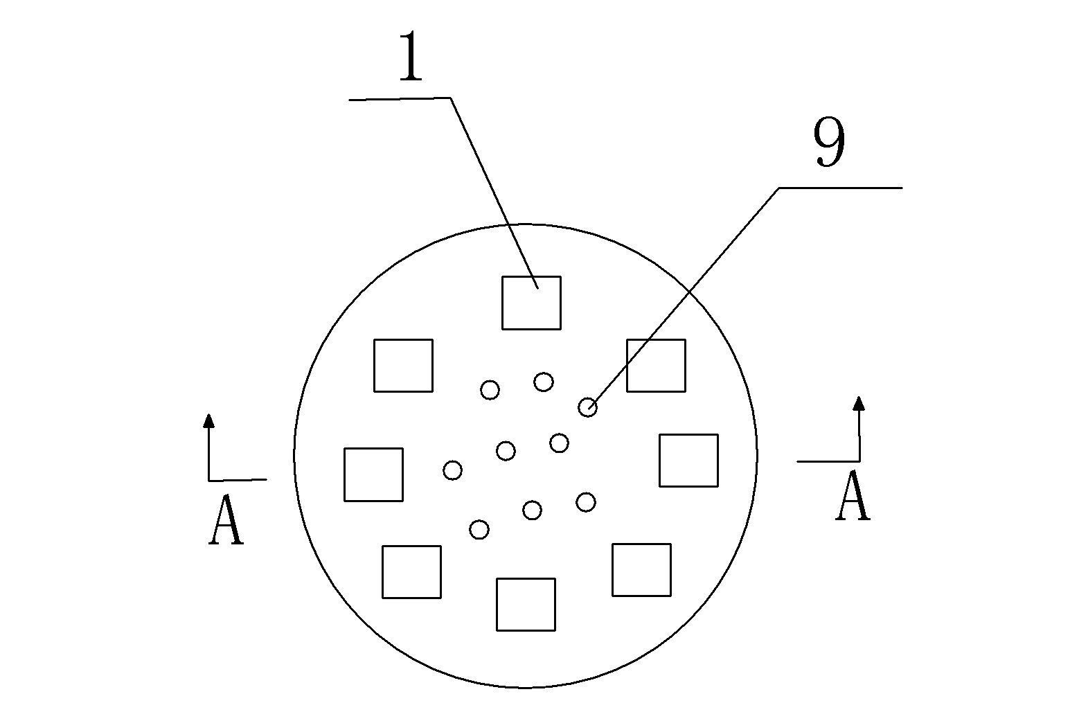
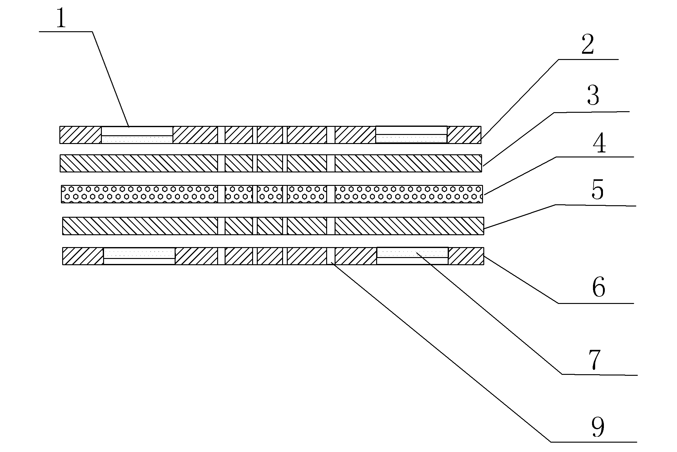
[0023] Such as figure 1 and figure 2 Shown: a double mosaic layer wax-free grinding and polishing template, the upper mosaic layer 2 of the double mosaic layer wax-free grinding and polishing template is provided with at least one film placement hole 1, in figure 1 Among them, the described hole 1 is a circular hole; figure 2 Among them, the sheet hole 1 is a rectangular hole; in the actual processing process, the shape of the sheet hole 1 can be processed and matched according to the shape of the material to be ground and polished; the lower mosaic layer 6 has a The same technical features of the mosaic layer 2, the wax-free grinding and polishing template of the double mosaic layer is provided with a diversion hole 9 for infiltrating the polishin...


PUM

PropertyMeasurementUnit
Diameteraaaaaaaaaa

Abstract

The invention relates to a wax-free grinding and polishing template with double inlaying layers. The grinding and polishing template is characterized by being a composite structure formed by five cylindrical laminar objects. The composite structure comprises a first layer, a second layer, a third layer, a fourth layer and a fifth layer from top to bottom; the first layer is an upper inlaying layer which is provided with at least one sheet placing hole; the second layer is an upper bonding layer; the third layer is a substrate layer; the fourth layer is a lower bonding layer; and the fifth layer is a lower inlaying layer which is provided with at least one sheet placing hole; the wax-free grinding and polishing template with double inlaying layers is provided with a guiding hole for permeation of a polishing liquid; and the diameter of guiding hole is 0.1-50mm. According to the wax-free grinding and polishing template, by adoption of double inlaying layers, the wax-free polishing efficiency is improved. Because a wax-free polishing pad is separated from an adsorbing pad, the deviation of the thickness of a silicon wafer product is reduced effectively, and the production cost is lowered effectively; and the wax-free grinding and polishing template with double inlaying layers has the characteristics of simple structure and convenience of processing.

Description

technical field [0001] The invention relates to the field of semiconductor material polishing devices, in particular to a wax-free grinding and polishing template with double mosaic layers applied to a double-sided polishing machine. Background technique [0002] In the processing of semiconductor materials, silicon wafers, sapphire and gallium arsenide, as the basic materials of common semiconductor devices and integrated circuits, often need to be polished, and the quality of the polishing technology will directly affect the quality of silicon wafers, sapphire and gallium arsenide. The surface quality of gallium arsenide and the performance of semiconductor devices. There are two main traditional polishing techniques: wax polishing and wax-free polishing. The wax technique is to bond and fix silicon wafers, sapphire or gallium arsenide to ceramic discs. On the flat plate, the polishing head drives the ceramic disc to rotate on the polishing cloth during polishing, and the ...

Claims


Application Information

Patent Timeline
IPC IPC(8): B24B37/22B24B37/26
Inventor 高如山
Owner 天津西美半导体材料有限公司
Features
  • Generate Ideas
  • Intellectual Property
  • Life Sciences
  • Materials
  • Tech Scout
  • Unparalleled Data Quality
  • Higher Quality Content
  • 60% Fewer Hallucinations
Learn More