Preparation method of delafossite type copper aluminum oxide infrared transparent conductive film

A transparent conductive film, infrared technology, applied in metal material coating process, vacuum evaporation plating, coating, etc., can solve the problems of opacity, achieve good transmittance, improve film quality, and stabilize deposition rate.

Inactive Publication Date: 2012-07-18
JILIN UNIV
View PDF2 Cites 4 Cited by
  • Summary
  • Abstract
  • Description
  • Claims
  • Application Information

AI Technical Summary

Problems solved by technology

It is widely used in flat panel display, touch screen and sensor window, but most of the current transparent conductive materials are n-type; in addition, most of the films currently used are only transparent in the visible light range, opaque and highly

Method used


Image

  • Preparation method of delafossite type copper aluminum oxide infrared transparent conductive film
  • Preparation method of delafossite type copper aluminum oxide infrared transparent conductive film
  • Preparation method of delafossite type copper aluminum oxide infrared transparent conductive film

Examples


Embodiment 1

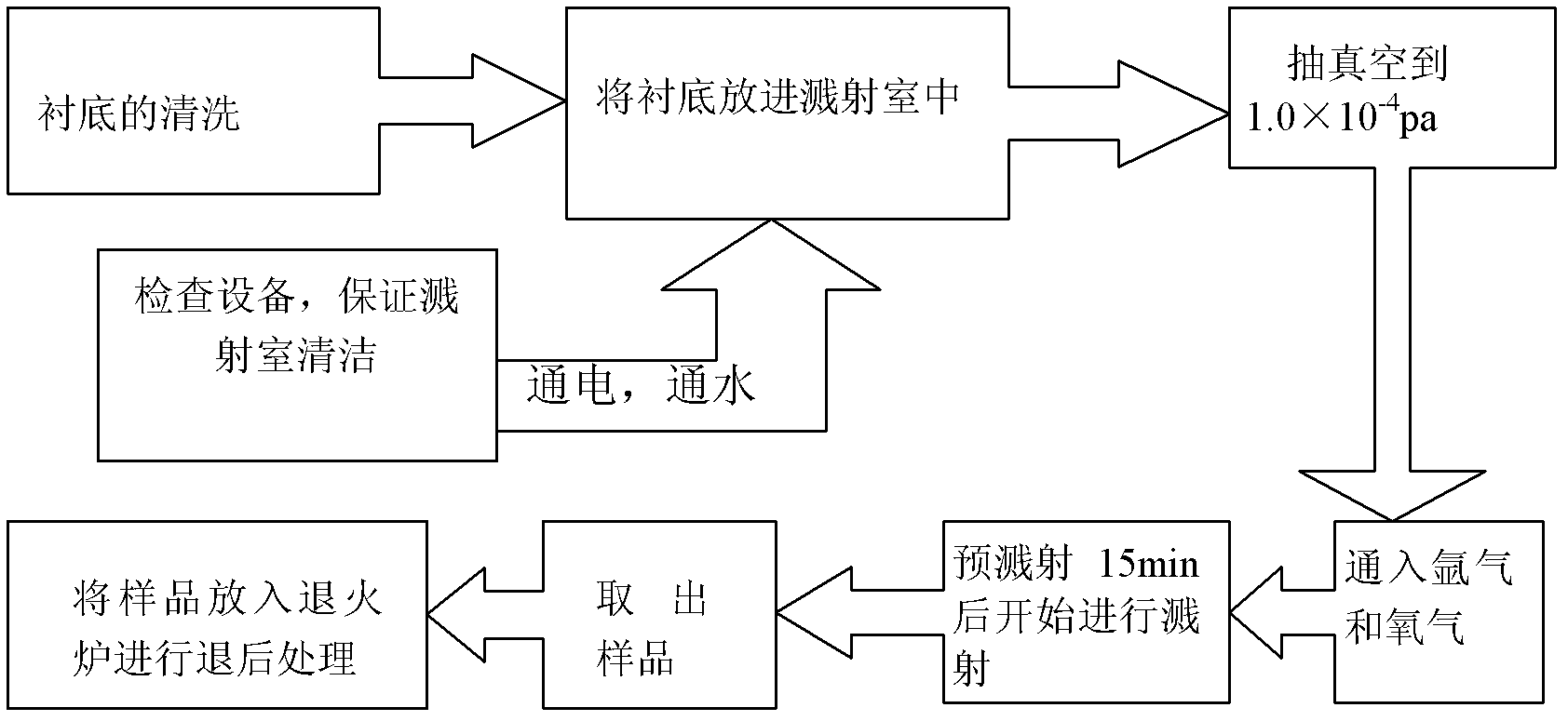
[0030] (1) Cleaning of the substrate

[0031] Cleaning of silicon (111) substrates: Clean with acetone solution (analytical grade) in an ultrasonic cleaner for 15 minutes at normal temperature and pressure, then soak in HF for 15 minutes, and finally rinse with deionized water for 5 minutes.

[0032] Cleaning of the sapphire substrate: Clean in an ultrasonic cleaner with acetone solution (analytical grade) for 15 minutes at normal temperature and pressure, then clean with an ethanol solution (analytic grade) in an ultrasonic cleaner for 15 minutes, and finally rinse with deionized water for 5 minutes.

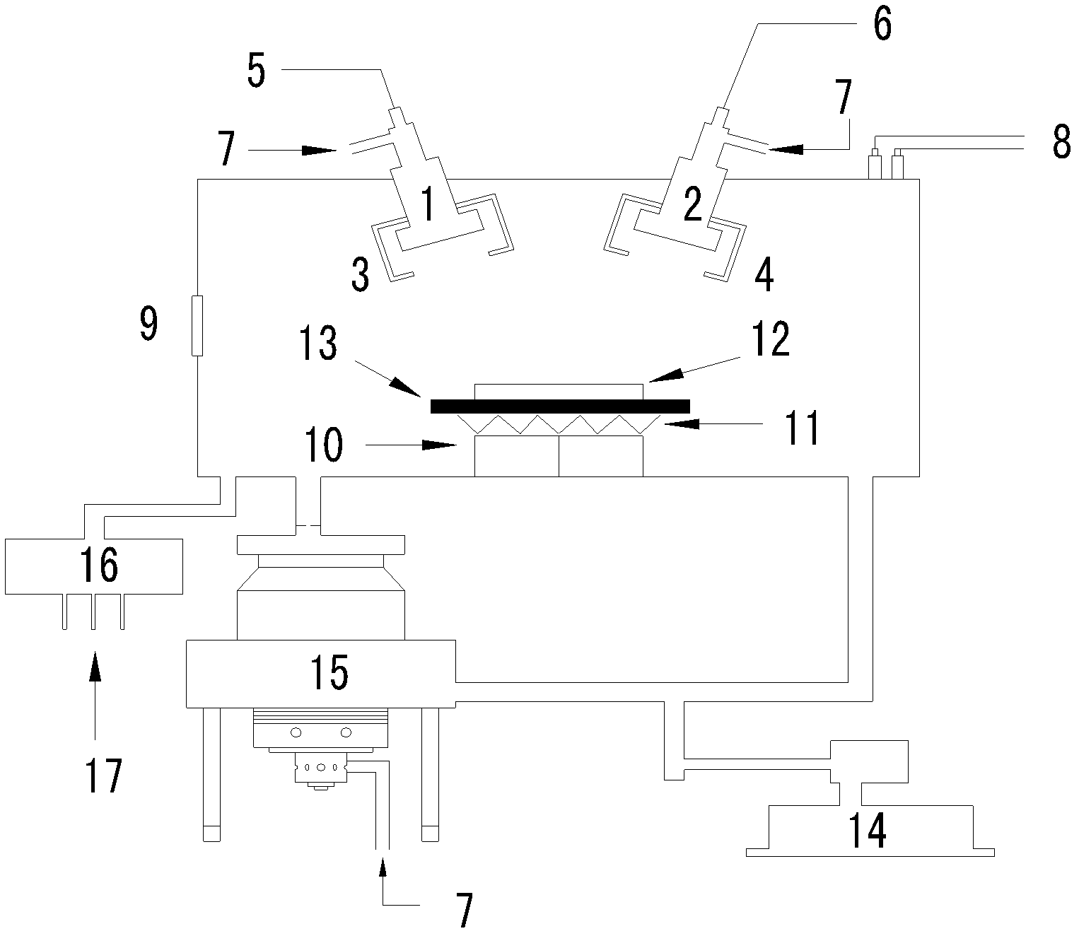
[0033] The two kinds of substrates were dried and placed in the sputtering chamber, where the thin films grown on the silicon substrates were used to test the structure and conductivity of the samples (such as Figure 4 and Figure 5 ), the film grown on the quartz substrate is used to measure the transmittance of the film (such as Figure 6 );

[0034] (2)CuAlO 2 film grow...

Embodiment 2

[0039] (1) Cleaning of the substrate

[0040] Cleaning of silicon (111) substrates: Clean with acetone solution (analytical grade) in an ultrasonic cleaner for 15 minutes at normal temperature and pressure, then soak in HF for 15 minutes, and finally rinse with deionized water for 5 minutes.

[0041] Cleaning of the sapphire substrate: Clean in an ultrasonic cleaner with acetone solution (analytical grade) for 15 minutes at normal temperature and pressure, then clean with an ethanol solution (analytic grade) in an ultrasonic cleaner for 15 minutes, and finally rinse with deionized water for 5 minutes.

[0042] Dry the two substrates and put them into the sputtering chamber, where the thin film grown on the silicon substrate is used to test the structure and conductivity of the sample, and the thin film grown on the quartz substrate is used to measure the transmittance of the thin film;

[0043] (2)CuAlO 2 film growth

[0044] The process is carried out in a high-vacuum multi...


PUM


Abstract

The invention relates to a preparation method of a nanoscale infrared transparent conductive film, in particular to a preparation method of an infrared transparent conductive film which is used in the infrared window and is transparent and conductive. The preparation method selects sapphire or silicon (111) as a substrate material for thin film growth; the preparation method of the thin film mainly adopts a high-vacuum magnetron sputtering technology; a co-target sputtering method is provided, wherein the target materials are respectively a Cu2O target and a Al2O3 target, or a Cu target and an Al target; and the obtained thin film is annealed in nitrogen at 500-600 DEG C for 3-5h to complete a preliminary chemical reaction, and then the thin film is annealed at a high temperature of 1000-1200 DEG C for 3-5h to completely react and crystallize. According to the preparation method, by adjusting the power of the two targets to control the compositions of the thin film, the problem of the one-target sputtering method that the ratio of Cu to Al can not be accurately controlled to be 1:1 so as to generate various oxides is solved; and the two-step annealing mode is adopted to avoid the loss of the related copper oxides caused by direct high-temperature annealing, thus the quality of the thin film can be increased.

Description

technical field [0001] The invention belongs to the field of infrared optical materials and electronic thin film materials, and in particular relates to a preparation method of a nano-scale infrared transparent conductive film, in particular to a preparation method of a transparent and conductive infrared transparent conductive film used for an infrared window. Background technique [0002] The transparent conductive film not only has light transmittance but also has good electrical conductivity. It is widely used in flat panel display, touch screen and sensor window, but most of the current transparent conductive materials are n-type; in addition, most of the films currently used are only transparent in the visible light range, opaque and highly reflective in the infrared light region rate, and the current infrared system also requires antistatic, defogging, dustproof and other functions, so it is necessary to prepare a conductive film that also has good transmittance in th...

Claims


Application Information

Patent Timeline
IPC IPC(8): C23C14/34C23C14/08
Inventor 王一丁曹峰陈君景董成军曹佳佳付强揣雅惠陈晨
Owner JILIN UNIV
Why Eureka
Try Eureka