Process for manufacturing micro-lens array with large numerical aperture

A technology of microlens array and numerical aperture, which is applied in the fields of lenses, optics, instruments, etc., can solve the problems of difficult large-area preparation, high cost, and unsatisfactory numerical aperture and other parameters, and achieve the effect of reducing costs

Inactive Publication Date: 2012-07-18
XI AN JIAOTONG UNIV
View PDF5 Cites 7 Cited by
  • Summary
  • Abstract
  • Description
  • Claims
  • Application Information

AI Technical Summary

Problems solved by technology

However, the current methods of manufacturing microlens arrays all have problems of high cost, difficulty in large-scale preparation, and unsatisfactory parameters such as numerical aperture, which are difficult to meet the needs of more and more fields for microlens arrays.

Method used


Image

  • Process for manufacturing micro-lens array with large numerical aperture
  • Process for manufacturing micro-lens array with large numerical aperture
  • Process for manufacturing micro-lens array with large numerical aperture

Examples


Embodiment Construction

[0030] The present invention is described in further detail below in conjunction with accompanying drawing:

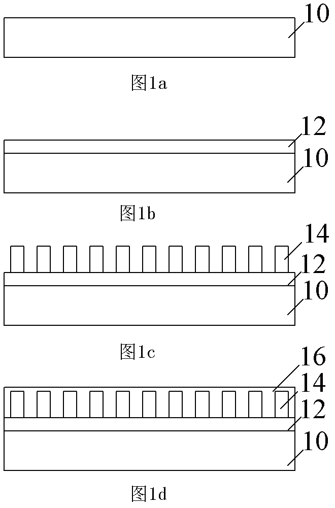
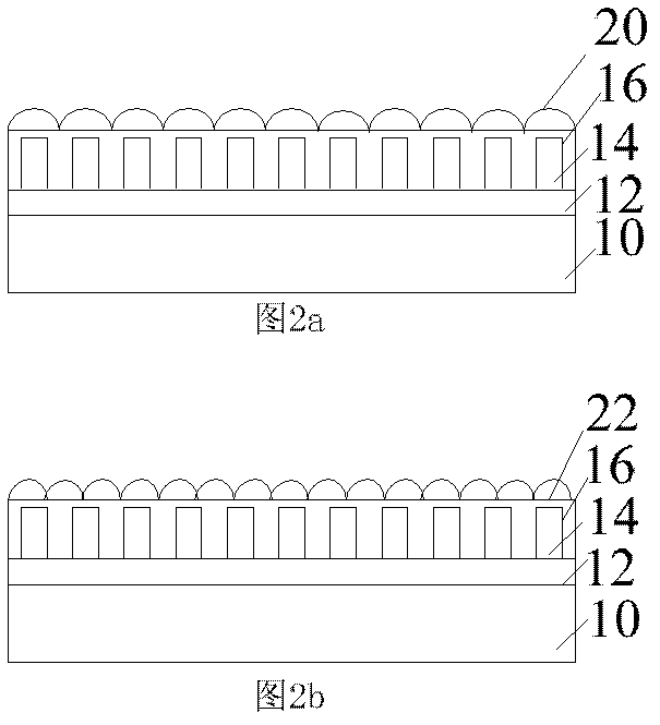
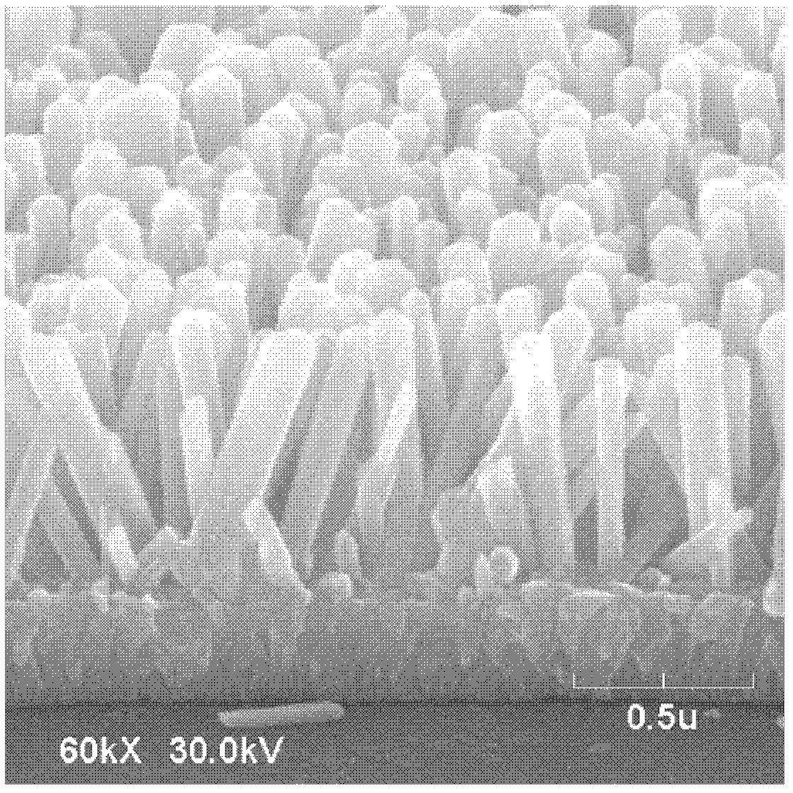
[0031] see Figure 1-4 , the technical process of preparing a large numerical aperture microlens array by inkjet printing disclosed in this patent includes the following steps:

[0032] (1) In the substrate cleaning step, the substrate glass is ultrasonically cleaned with detergent, deionized water and acetone-ethanol solution, and then the substrate is dried under an infrared lamp.

[0033] (2) if figure 1 As shown in b, a layer of ZnO amethyst layer is sputtered on the glass slide by radio frequency magnetron sputtering at room temperature. After the sputtering speed (power) is adjusted, the longer the sputtering time, the thicker the obtained amethyst layer; In this embodiment, the sputtering time is 5 minutes, and the thickness of the purple gold layer is about 100 nanometers.

[0034] (3) if figure 1 As shown in b, ZnO nanocolumns are grown in a water bath on ...


PUM

PropertyMeasurementUnit
thicknessaaaaaaaaaa

Abstract

The invention discloses a process for manufacturing a micro-lens array with a large numerical aperture, which comprises the following steps (a) manufacturing a zinc oxide nanometer column; (b) manufacturing an octafluorocyclobutane (C4F8) layer on the surface of the zinc oxide nanometer column; (c) manufacturing a micro-lens in a spray ink printing mode; and (d) curing the micro-lens and enabling the micro-lens array obtained in the step (b) to be cured through a mode of ultraviolet light source exposure and substrate heating. The method greatly reduces cost of the existing graphical technology, has potential of large-area manufacture simultaneously, and remarkably improves the numerical aperture of the micro-lens array. In addition, the spray ink printing is the process of natural dropping and forming of liquid drops, roughness of the surface of the manufactured lens is low, and errors including noises and the like can be removed when the lens is actually used.

Description

technical field [0001] The invention relates to a manufacturing process of a microlens array, in particular to a manufacturing process of a microlens with a large numerical aperture. Background technique [0002] A lens is one of the most basic units that constitute an optical system. It is formed by a transparent medium surrounded by two refractive surfaces, and is used to transmit and refract incident light, so that the light wavefront is modulated to achieve a specific optical effect. Optical components are indispensable and important components in optical instruments and optoelectronic systems. As one of the important devices in the field of micro-optics, micro-lens arrays are widely used in optical fiber coupling, beam shaping, integrated imaging, and optical neural networks. [0003] In recent years, the manufacturing technology of microlenses and microlens arrays has developed rapidly. At present, a large number of researchers at home and abroad are engaged in the r...

Claims


Application Information

Patent Timeline
Patent Type & Authority Applications(China)
IPC IPC(8): G02B3/00
Inventor 王莉罗钰丁玉成魏慧芬卢秉恒
Owner XI AN JIAOTONG UNIV
Why Eureka
Try Eureka