Manufacturing method of gate controlled diode semiconductor device

A technology for gate-controlled diodes and manufacturing methods, which is applied in the manufacture of gate-controlled diode semiconductor devices and the field of semiconductor device manufacturing, can solve problems such as driving current reduction, and achieve large driving currents, small sub-threshold swings, and low manufacturing costs Effect

Inactive Publication Date: 2012-07-18
FUDAN UNIV
View PDF5 Cites 7 Cited by
  • Summary
  • Abstract
  • Description
  • Claims
  • Application Information

AI Technical Summary

Problems solved by technology

However, while the leakage current is reduced, the driving current of the tunneling field effect transistor is also reduced. Therefore, the tunneling field effect transistor is still facing the challenge of how to increase the driving current.

Method used


Image

  • Manufacturing method of gate controlled diode semiconductor device
  • Manufacturing method of gate controlled diode semiconductor device
  • Manufacturing method of gate controlled diode semiconductor device

Examples


Embodiment Construction

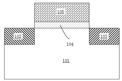
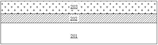
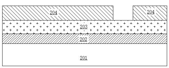
[0016] Hereinafter, an exemplary embodiment of the present invention will be described in detail with reference to the accompanying drawings. In the figure, for convenience of description, the thickness of layers and regions are enlarged or reduced, and the size shown does not represent the actual size. Although these figures do not completely accurately reflect the actual size of the device, they still completely reflect the mutual position between the regions and the constituent structures, especially the upper and lower and adjacent relationships between the constituent structures.

[0017] The reference figure is a schematic diagram of an idealized embodiment of the present invention. The embodiment shown in the present invention should not be regarded as limited to the specific shape of the area shown in the figure, but includes the resulting shape, such as deviations caused by manufacturing. For example, the curves obtained by etching usually have the characteristics of ben...


PUM


Abstract

The invention belongs to the technical field of the manufacture of semiconductor devices, and specifically relates to a manufacturing method of a gate controlled diode semiconductor device. The manufacturing method is characterized in that a low temperature technology is adopted to prepare the gate controlled diode semiconductor device, the technical process is simple, the manufacturing cost is low, and the manufactured gate control diode device has the advantages of large drive current and small sub-threshold amplitude. The manufacturing method of the gate controlled diode semiconductor device provided by the invention is particularly suitable for panel display and a read-write device of a phase change memorizer and manufacture based on the semiconductor device of a flexible substrate.

Description

Technical field [0001] The invention belongs to the technical field of semiconductor device manufacturing, in particular to a method of manufacturing a semiconductor device, and in particular to a method of manufacturing a gate-controlled diode semiconductor device. Background technique [0002] With the continuous development of integrated circuit technology, the size of metal-oxide-silicon field effect transistors (MOSFETs) is getting smaller and smaller, and the density of transistors on a unit array is getting higher and higher. Today's integrated circuit device technology node is around 45 nanometers, and the leakage current between the source and drain of the MOSFET increases rapidly as the channel length shrinks. Moreover, the minimum sub-threshold swing (SS) of the traditional MOSFET is limited to 60mv / dec, which limits the switching speed of the transistor. On some chips with higher integration density, reducing the size of the device means a larger SS value, and for hi...

Claims


Application Information

Patent Timeline
Patent Type & Authority Applications(China)
IPC IPC(8): H01L21/329
CPCH01L29/7391H01L29/0653H01L29/267H01L29/517H01L29/66356
Inventor 王鹏飞林曦孙清清张卫
Owner FUDAN UNIV
Why Eureka
Try Eureka