Mixed bonding structure for three-dimension integration and bonding method for mixed bonding structure

A three-dimensional integration and hybrid bonding technology, which is applied in semiconductor/solid-state device components, semiconductor devices, electrical components, etc., can solve the problems of high pressure required for bonding, small interconnection pitch, damage, etc., and achieve compact structure , The process is convenient to operate, and the effect of avoiding open circuit and reliability problems

Active Publication Date: 2012-07-18
NAT CENT FOR ADVANCED PACKAGING
View PDF2 Cites 38 Cited by
  • Summary
  • Abstract
  • Description
  • Claims
  • Application Information

AI Technical Summary

Problems solved by technology

[0003] The advantage of using metal bump interconnection in three-dimensional integrated circuits is that a small interconnection pitch can be obtained, and Cu-Cu bump bonding can obtain excellent electrical performance and reliability; the disadvantage is that the metal bumps are required to have a high Flatness, usually requires high bonding temperature (>300°C), and special surface treatment to remove oxides on the metal surface
Further, due to the increase in interconnection density, the pressure required for bonding is increasing, which will cause damage to 3D integration, especially thin chips with TSV structures

Method used


Image

  • Mixed bonding structure for three-dimension integration and bonding method for mixed bonding structure
  • Mixed bonding structure for three-dimension integration and bonding method for mixed bonding structure
  • Mixed bonding structure for three-dimension integration and bonding method for mixed bonding structure

Examples


Embodiment Construction

[0045] The present invention will be further described below in conjunction with specific drawings and embodiments.

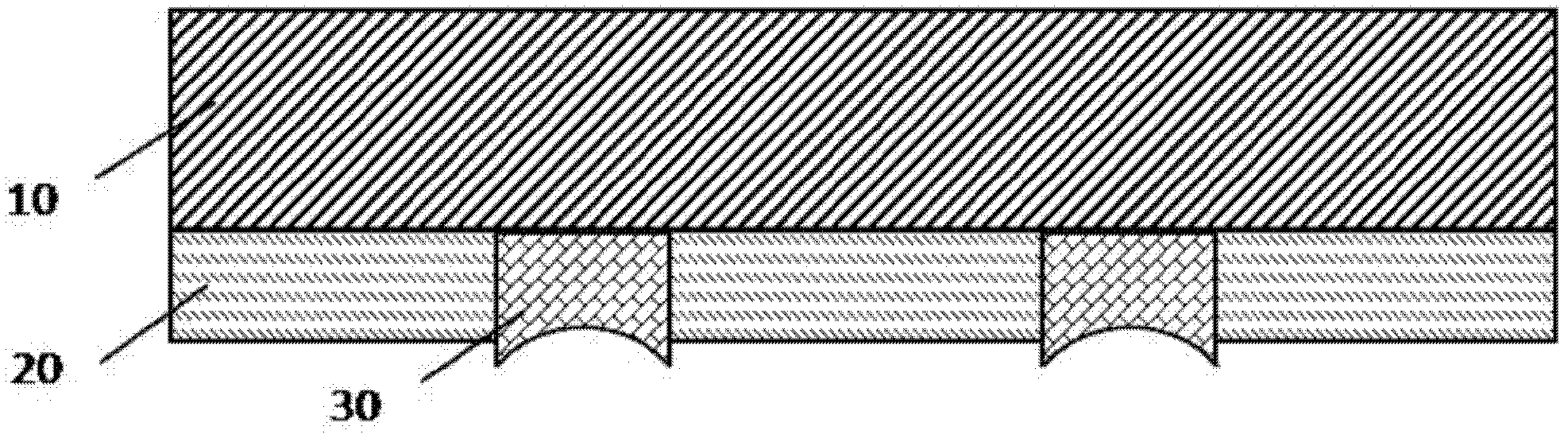
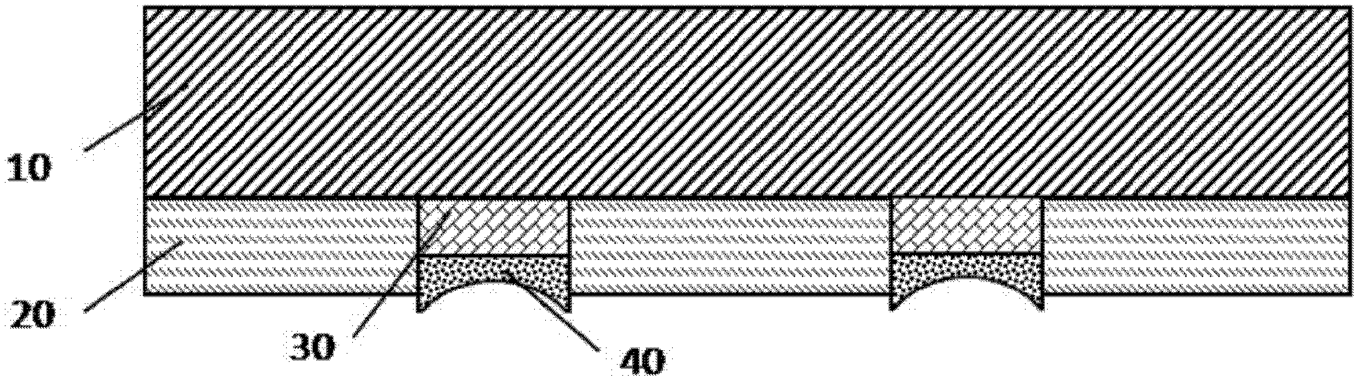
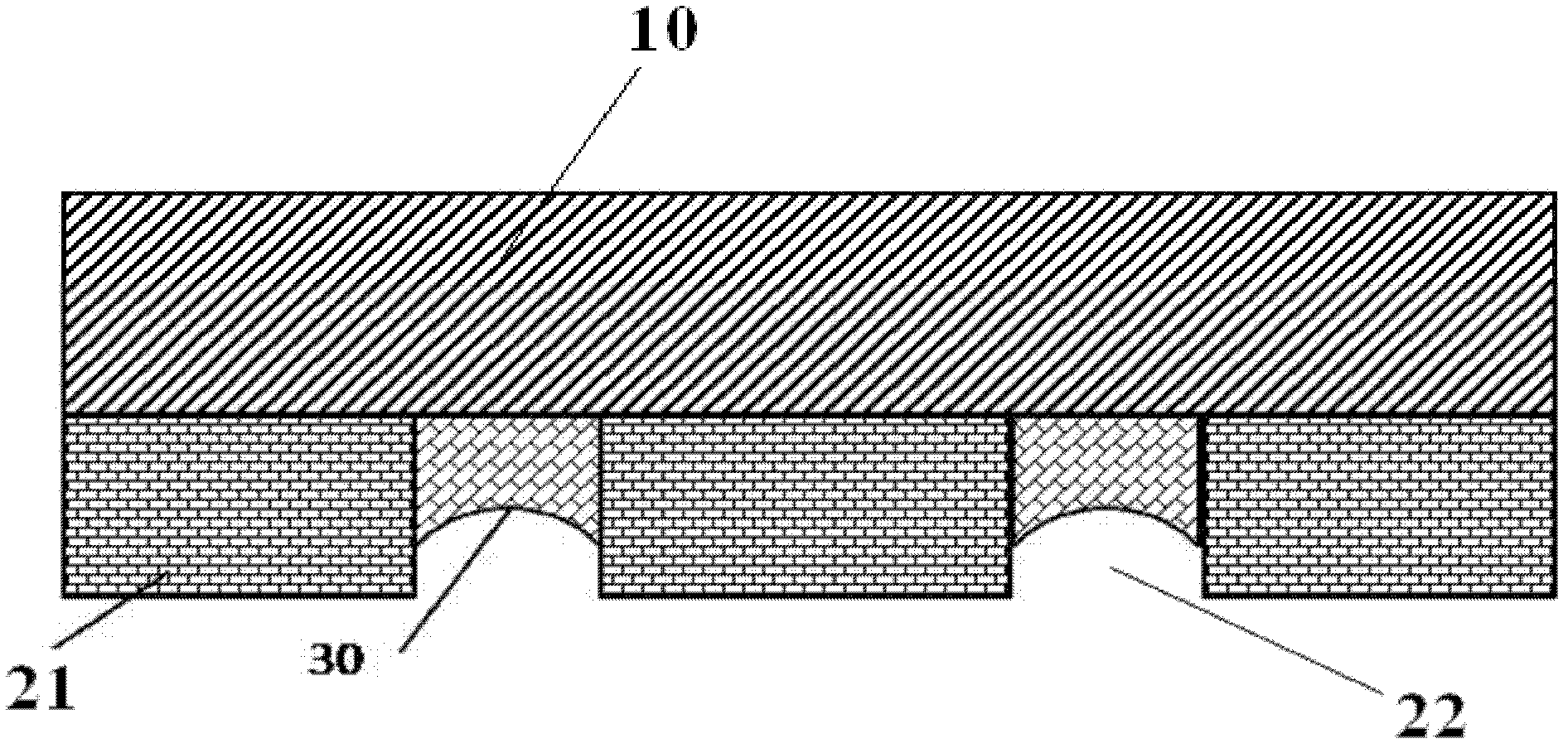
[0046] like figure 1 and figure 2 Shown: in order to avoid the problem of disconnection and reliability caused in the existing bonding process, the present invention includes a first bonding body 1, and the first bonding body 1 includes a first substrate 10; the first substrate 10 is provided with a The first substrate 10 is electrically connected to the bonding interconnection metal, and the other end of the bonding interconnection metal corresponding to the first substrate 10 is indented to form a cavity 31, that is, a cavity 31 is formed corresponding to the bonding interconnection metal The end of the bump 31 forms a bump top edge 60, and the surface of the first substrate 10 corresponding to the bonding interconnection metal is covered with a first dielectric adhesion layer 20, which surrounds the bonding interconnection. The height of the first dielect...


PUM


Abstract

The invention relates to a mixed bonding structure for three-dimension integration and a bonding method for the mixed bonding structure. The mixed bonding structure for the three-dimension integration comprises a first substrate. The first substrate is provided with bonding interconnection metal electrically connected with the first substrate; the other end part of the bonding interconnection metal, which is correspondingly connected with the first substrate, is sunk to form a cavity; a first dielectric adhesion layer covers at the periphery of the bonding interconnection metal on the first substrate; the bonding interconnection metal is encircled by the first dielectric adhesion layer; and the first dielectric adhesion layer is lower than the edge of the bonding interconnection metal. According to the mixed bonding structure for the three-dimension integration, the first dielectric adhesion layer is lower than the edge of the top part of a salient point, and when bonding is performed under the pressure action, the edge of the top part of the salient point is bonded with a pad of a second substrate, and thereby, the dielectric adhesion layer can be stopped entering the surface of the bonding interconnection metal, which is bonded with the pad, and the open circuit problem and the reliability problem can be avoided. The mixed bonding structure for the three-dimension integration is compact in structure and is convenient in process operation.

Description

technical field [0001] The invention relates to a hybrid bonding structure and a bonding method thereof, in particular to a hybrid bonding structure for three-dimensional integration and a bonding method thereof, belonging to the technical field of integrated circuits. Background technique [0002] The core technologies of 3D integrated circuits include TSV (Through Silicon Via) fabrication, wafer thinning, thin wafer handling, and bonding technologies. These technologies are all extremely challenging. The bonding technology includes chip-to-chip, chip-to-wafer and wafer-to-wafer bonding. For the above three bonding technologies, there are two materials for electrical interconnection, one is metal bumps, such as Cu, Au, etc.; the other is solder bump interconnection, such as Sn, In, etc. [0003] The advantage of using metal bump interconnection in three-dimensional integrated circuits is that a small interconnection pitch can be obtained, and Cu-Cu bump bonding can obtain...

Claims


Application Information

Patent Timeline
Patent Type & Authority Applications(China)
IPC IPC(8): H01L23/488H01L21/603
CPCH01L2224/80357H01L2224/05557H01L2224/05567H01L2224/80896H01L2224/0391H01L2224/08147H01L2224/05571H01L2224/05572H01L2224/80895H01L2224/80345H01L24/08H01L24/80H01L2224/80201H01L23/488H01L2224/80986H01L24/05H01L2924/00014H01L2924/14H01L2224/80035H01L2224/80935H01L2224/80359H01L2224/8034H01L2224/08145H01L2924/00012H01L2224/05552H01L2924/00
Inventor 于大全
Owner NAT CENT FOR ADVANCED PACKAGING
Why Eureka
Try Eureka