Method for reducing converted currents of resistive random access memories

A resistive variable memory and current technology, applied in static memory, digital memory information, information storage, etc., can solve the problems of poor resistance value consistency of resistive variable memory, increase of low-resistance state current, too thick and too many channels, etc., to achieve Improve uniformity, reduce power consumption, and reduce the effect of switching current

Active Publication Date: 2012-07-25
PEKING UNIV
View PDF4 Cites 1 Cited by
  • Summary
  • Abstract
  • Description
  • Claims
  • Application Information

AI Technical Summary

Problems solved by technology

However, the formation of conductive channels in the forming process has great randomness, which leads to poor resistance consistency of the resistance variable memory, and the forming process is generally not easy to control, resulting in too thick and too many channels formed, thus Increase the current in the low-impedance state

Method used


Image

  • Method for reducing converted currents of resistive random access memories
  • Method for reducing converted currents of resistive random access memories
  • Method for reducing converted currents of resistive random access memories

Examples


Embodiment 1

[0027] The memory array chip is placed in a closed cavity, and the temperature of the cavity is raised to 85° C. to 250° C. Apply scanning voltage signals to all RRAMs in the array to complete the Forming process. The scanning voltage starts from 0V and ends at 2V-10V. The scanning voltage increases by 0.01V-0.05V each time, and each voltage value is maintained for 1us-1ms. At the same time, limit the current, the current is 50nA ~ 50uA. The specific values ​​of the heating temperature, voltage, and current are different from the metal and oxide materials used in the resistive variable memory. The heating temperature is preferably the above-mentioned 85°C to 250°C, such as: 90°C, 100°C, 150°C or 200°C .

Embodiment 2

[0029] The prepared 1T-1R memory array chip is placed on a platform, and the temperature of the platform is raised to 85° C. to 250° C. Apply a scanning voltage signal to all resistive memory cells in the array to complete the forming process. The scanning voltage starts from 0V and ends at 2V-10V. The scanning voltage increases by 0.01V-0.05V each time, and each voltage value is maintained for 1us-1ms. At the same time, the gate voltage of the pass transistor connected in series with the resistive variable memory is adjusted so that the saturation current of the transistor is 50nA-50uA.

Embodiment 3

[0031] The memory array chip is placed in a closed cavity, and the temperature of the cavity is raised to 85° C. to 250° C. The forming process is completed by applying scanning current signals to all RRAMs in the array. The scanning current starts from 0A and increases linearly to 50nA-50uA. The scanning current increases by 0.5nA-50nA each time, and each current value is maintained for 1us-1ms.

[0032] The following introduces the principle why the method of the present invention can reduce the transition current of the RRAM and improve the uniformity of the device.

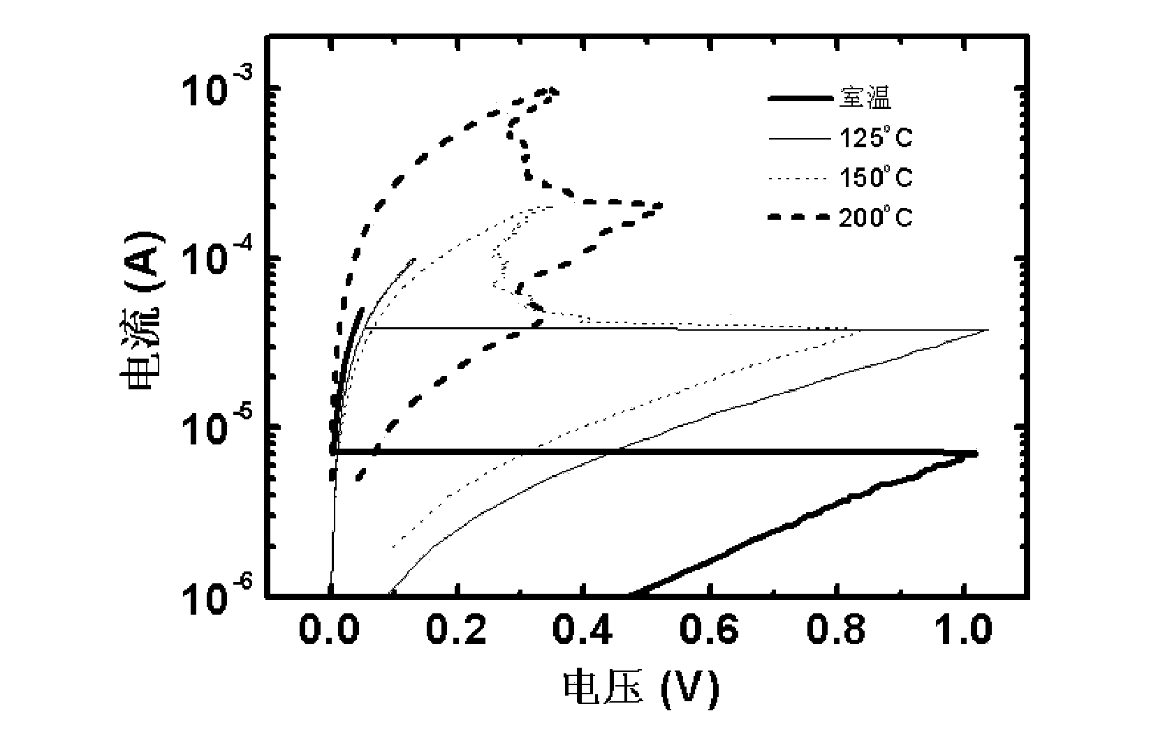
[0033] The forming process of resistive memory at room temperature generally exhibits properties similar to avalanche breakdown, such as figure 1 As shown, the resistance of the device shows a sudden change from the initial resistance to low resistance during Forming at room temperature. No matter what current limiting method is used, this avalanche process cannot be prevented, so the current limiting effect a...


PUM


Abstract

The invention discloses a method for reducing converted currents of resistive random access memories, relating to the technical field of microelectronic semiconductors. The method is implemented through completing an electrical forming process under the condition of heating all resistive random access memories in a memory array. By using the method disclosed by the invention, the converted currents of resistive random access memories are significantly reduced, thereby reducing the power consumption, and improving the reliability of devices; and low-impedance-state resistance values can be effectively controlled, thereby enhancing the resistance value uniformity of devices.

Description

technical field [0001] The invention relates to the technical field of microelectronics and semiconductors, in particular to a method for reducing the switching current of a resistive variable memory. Background technique [0002] Resistive-RAM (RRAM) is a new type of non-volatile memory that uses controllable resistance changes to store data. This kind of memory has the advantages of high speed (<1 ns), low voltage (<1.5V), high storage density, multi-value storage in one storage unit, and easy integration. It is a strong competitor for the next generation of semiconductor memory. The resistive variable memory is generally made of a metal-resistive layer-metal sandwich structure, in which the two outer layers of metal are electrodes, and the middle resistive layer is generally a metal oxide, which has the function of variable resistance. The working principle of the resistive variable memory is to apply voltages of different magnitudes or polarities across the resist...

Claims


Application Information

Patent Timeline
Patent Type & Authority Applications(China)
IPC IPC(8): G11C11/56
Inventor 高滨康晋锋刘力锋
Owner PEKING UNIV
Why Eureka
Try Eureka