Method for reducing switching current of resistive variable memory
A resistive variable memory and current technology, applied in static memory, digital memory information, information storage, etc., can solve the problems of poor resistance value consistency of resistive variable memory, increase of low-resistance state current, too thick and too many channels, etc., to achieve Improve uniformity, reduce power consumption, and reduce the effect of switching current
- Summary
- Abstract
- Description
- Claims
- Application Information
AI Technical Summary
Problems solved by technology
Method used
Image
Examples
Embodiment 1
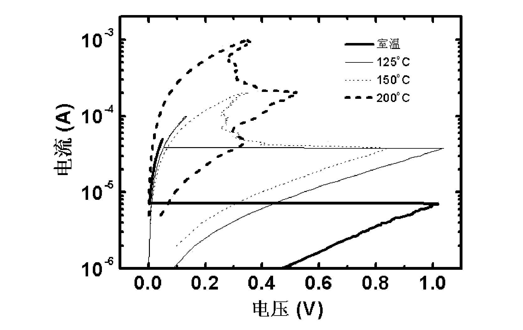
[0027] The memory array chip is placed in a closed cavity, and the temperature of the cavity is raised to 85° C. to 250° C. Apply scanning voltage signals to all RRAMs in the array to complete the Forming process. The scanning voltage starts from 0V and ends at 2V-10V. The scanning voltage increases by 0.01V-0.05V each time, and each voltage value is maintained for 1us-1ms. At the same time, limit the current, the current is 50nA ~ 50uA. The specific values of the heating temperature, voltage, and current are different from the metal and oxide materials used in the resistive variable memory. The heating temperature is preferably the above-mentioned 85°C to 250°C, such as: 90°C, 100°C, 150°C or 200°C .
Embodiment 2
[0029] The prepared 1T-1R memory array chip is placed on a platform, and the temperature of the platform is raised to 85° C. to 250° C. Apply a scanning voltage signal to all resistive memory cells in the array to complete the forming process. The scanning voltage starts from 0V and ends at 2V-10V. The scanning voltage increases by 0.01V-0.05V each time, and each voltage value is maintained for 1us-1ms. At the same time, the gate voltage of the pass transistor connected in series with the resistive variable memory is adjusted so that the saturation current of the transistor is 50nA-50uA.
Embodiment 3
[0031] The memory array chip is placed in a closed cavity, and the temperature of the cavity is raised to 85° C. to 250° C. The forming process is completed by applying scanning current signals to all RRAMs in the array. The scanning current starts from 0A and increases linearly to 50nA-50uA. The scanning current increases by 0.5nA-50nA each time, and each current value is maintained for 1us-1ms.
[0032] The following introduces the principle why the method of the present invention can reduce the transition current of the RRAM and improve the uniformity of the device.
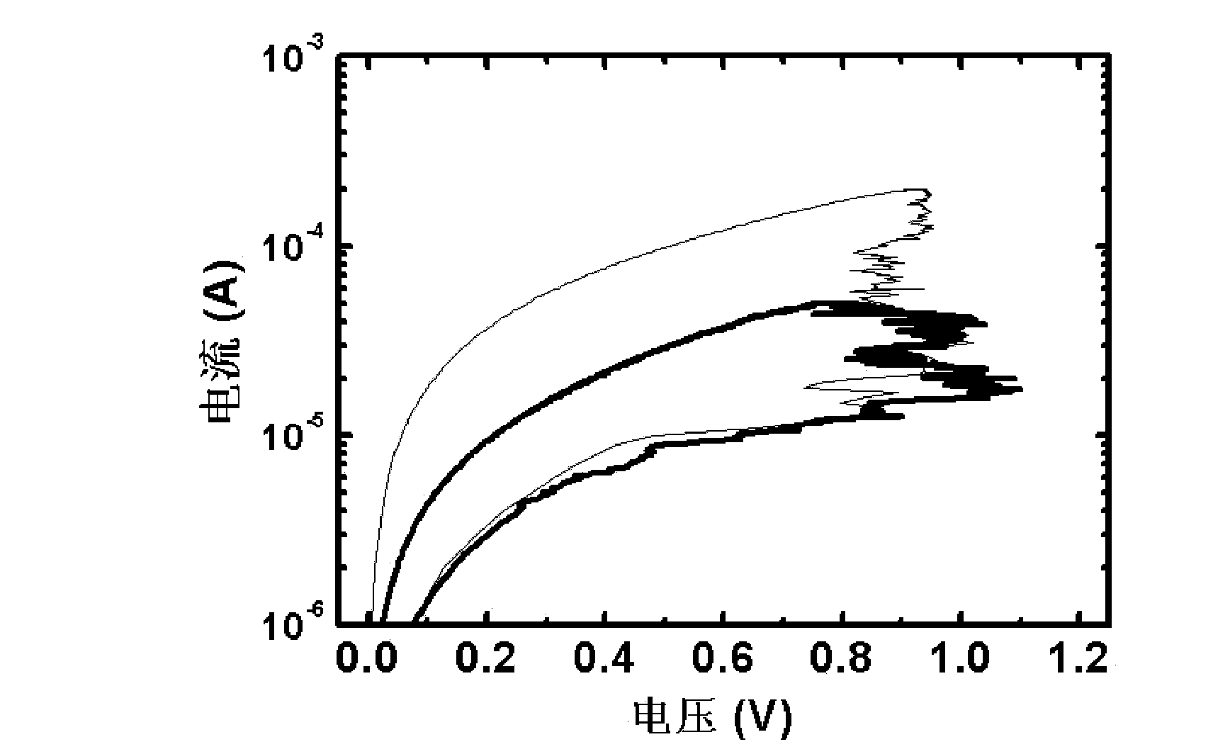
[0033] The forming process of resistive memory at room temperature generally exhibits properties similar to avalanche breakdown, such as figure 1 As shown, the resistance of the device shows a sudden change from the initial resistance to low resistance during Forming at room temperature. No matter what current limiting method is used, this avalanche process cannot be prevented, so the current limiting effect a...
PUM
 Abstract
Description
Claims
Application Information


