MOS element manufacturing method for reducing damage caused by hot carriers injection

A MOS device, injection damage technology, applied in semiconductor/solid-state device manufacturing, semiconductor devices, electrical components, etc., can solve problems such as threshold voltage degradation, MOS device failure, energy bond breakage, etc., to reduce damage, reduce gate The effect of polar current

Inactive Publication Date: 2012-07-25
SHANGHAI HUALI MICROELECTRONICS CORP
View PDF4 Cites 1 Cited by
  • Summary
  • Abstract
  • Description
  • Claims
  • Application Information

AI Technical Summary

Problems solved by technology

Hot carriers will break the energy bond at the interface between the silicon substrate and the silicon dioxide gate oxygen, and generate interface states at the interface between the silicon substrate and the silicon dioxide gate oxygen, resulting in device performance, such as threshold voltage, transconductance, and linearity. The degradation of the current in the region / saturation region will eventually cause the failure of the MOS device

Method used


Image

  • MOS element manufacturing method for reducing damage caused by hot carriers injection
  • MOS element manufacturing method for reducing damage caused by hot carriers injection
  • MOS element manufacturing method for reducing damage caused by hot carriers injection

Examples


Embodiment Construction

[0013] In order to make the above objects, features and advantages of the present invention more comprehensible, specific implementations of the present invention will be described in detail below in conjunction with the accompanying drawings.

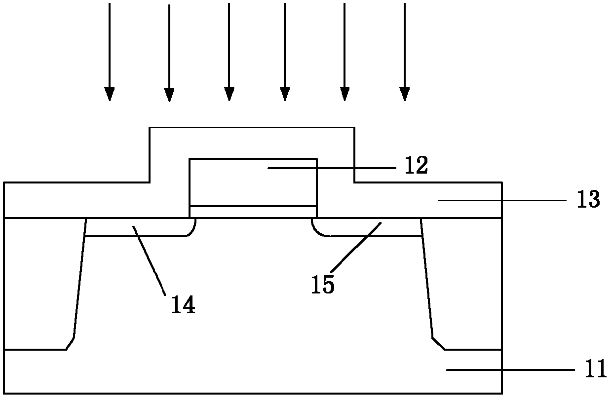
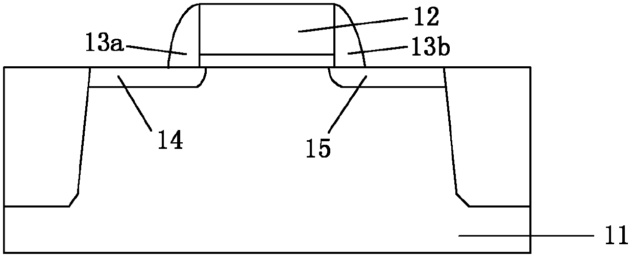
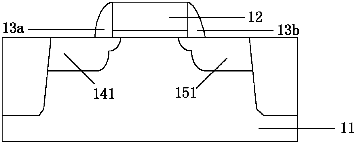
[0014] Please refer to Figure 2A-Figure 2F , taking the NMOS device in the CMOS transistor process as an example, the MOS device manufacturing method for reducing hot carrier injection damage of the present invention includes:

[0015] First, if Figure 2A As shown, a gate structure 22 is formed on a substrate 21, and the substrate 21 includes a source region and a drain region. The source region refers to the source extension region and the source heavily doped region to be formed later region, similarly, the drain region refers to the region where the drain extension region and the heavily doped drain region will be formed subsequently;

[0016] Then, if Figure 2B As shown, the gate structure 22 is used as a mask, and the substr...


PUM


Abstract

The invention discloses a MOS element manufacturing method for reducing damage caused by hot carriers injection; a photoresist layer is formed on a lateral wall deposition layer above a drain region; a method that neutral ions process ion injection to the lateral wall deposition layer above a source region is used, thus, a cross section width of an etched source lateral wall is relatively small; and the cross section width of a drain lateral wall is relatively increased. When voltage is added to grid, the strength of a longitudinal electric field generated on the drain is weakened; therefore, holes of electronic hole pairs generated by carriers collision accelerated by a transverse electric field will be injected into the grid under the action of a relatively weak longitudinal electric field; thus, grid current formed by injecting the hot carrier is reduced; and damage of hot carriers injection of semiconductors is reduced.

Description

technical field [0001] The invention relates to the field of semiconductor manufacturing, in particular to a MOS device manufacturing method for reducing hot carrier injection damage. Background technique [0002] The hot carrier effect is an important failure mechanism of MOS (metal oxide semiconductor) devices. With the shrinking of the size of MOS devices, the hot carrier injection effect of the devices becomes more and more serious. Taking a PMOS (P-type metal oxide semiconductor) device as an example, the holes in the channel are accelerated under the action of a high lateral electric field between the drain and source to form high-energy carriers, which collide with the silicon lattice. Generate ionized electron-hole pairs, the electrons are collected by the substrate to form a substrate current, most of the holes generated by the collision flow to the drain, but some holes are injected into the gate under the action of the vertical electric field The formation of gat...

Claims


Application Information

Patent Timeline
Patent Type & Authority Applications(China)
IPC IPC(8): H01L21/266H01L21/336
CPCH01L29/7835H01L29/66659
Inventor 俞柳江
Owner SHANGHAI HUALI MICROELECTRONICS CORP
Why Eureka
Try Eureka