A kind of semiconductor device with super junction structure and its manufacturing method

A semiconductor and device technology, applied in the field of semiconductor devices with a superjunction structure and their fabrication, can solve the problems affecting the conduction performance of the device, low saturation current, and large on-resistance of the device, etc.

Active Publication Date: 2021-01-15
汇佳网(天津)科技有限公司
View PDF4 Cites 0 Cited by
  • Summary
  • Abstract
  • Description
  • Claims
  • Application Information

AI Technical Summary

Problems solved by technology

At present, in order to improve the withstand voltage performance of devices, super-junction structures are widely used in semiconductor devices. Super-junction structures can effectively ensure device withstand voltage performance, save device area, and reduce production costs. However, the limitations of traditional super-junction structures cannot Give full play to its high performance advantages, which seriously affects the conduction performance of the device. Therefore, the prior art has technical problems of large device conduction resistance and low saturation current

Method used


Image

  • A kind of semiconductor device with super junction structure and its manufacturing method
  • A kind of semiconductor device with super junction structure and its manufacturing method
  • A kind of semiconductor device with super junction structure and its manufacturing method

Examples


Embodiment 1

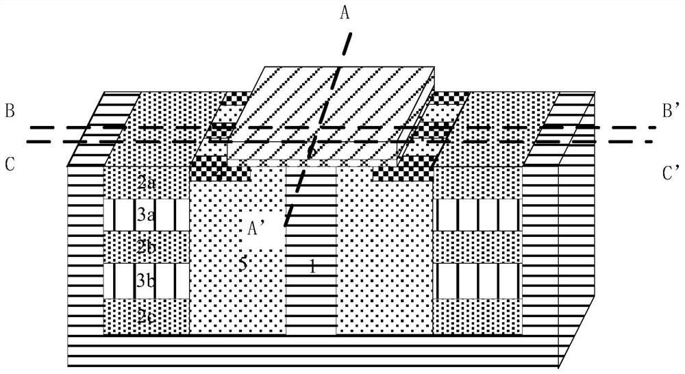
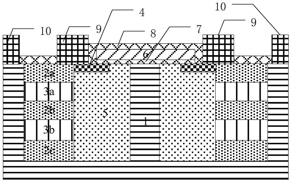
[0045] see Figure 1 to Figure 4 , a three-dimensional structure diagram and an internal cross-sectional diagram of a semiconductor device with a superjunction structure provided by an embodiment of the present invention. A semiconductor device with a superjunction structure provided by an embodiment of the present invention includes: an N-type substrate (not shown in the figure), an N+ region 1, a P-body region 5, a PN alternating superjunction region, and an N+ source region 4 , gate oxide layer 7, polysilicon gate 6, dielectric layer isolation 8, device source metal 9 and device drain metal 10. Wherein, the N+ region is an electron drift region composed of a central region, a bottom region and a side region. The cross-section of the side area is "mouth", the cross-section of the central area is "one", located in the center of the side area, and the bottom area is square, located at the bottom of the device.

[0046] The top of the N-type substrate is connected to the bott...

Embodiment 2

[0059] A method for manufacturing a semiconductor device with a super junction structure provided by an embodiment of the present invention includes:

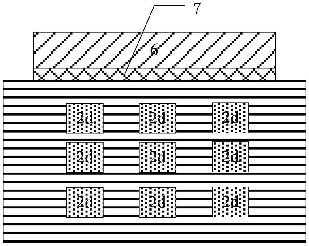
[0060] Step S1: providing an N-type substrate, forming an N+ epitaxial layer on the upper surface of the N-type substrate, forming a P- epitaxial layer on the upper surface of the N+ epitaxial layer, and performing surface planarization after epitaxy. see Figure 6 , a product schematic diagram of step S1 in the method for manufacturing a semiconductor device with a super junction structure provided by an embodiment of the present invention.

[0061] Step S2: forming deep trenches on both sides of the P- epitaxial layer, the bottom of the deep trenches extending to the upper surface of the N+ epitaxial layer. see Figure 7 , a product schematic diagram of step S2 in the method for manufacturing a semiconductor device with a super junction structure provided by an embodiment of the present invention.

[0062] Step S3: forming...


PUM

PropertyMeasurementUnit
widthaaaaaaaaaa

Abstract

The invention, which relates to the technical field of semiconductor chips, provides a semiconductor device with a super-junction structure and a manufacturing method thereof. The semiconductor devicecomprises an N type substrate, an N+ region, a P-body region, an PN alternating super-junction region, an N+ source region, a gate oxidation layer, a polycrystalline silicon gate, a dielectric layerisolation unit, a device source metal unit, and a device drain metal unit. P+ layers and N+ layers are arranged alternately and horizontally at intervals in the PN alternating super-junction region; and a super-junction P type-column array group formed by super-junction P type columns is arranged inside the central region of the N+ region horizontally. According to the invention, technical problems of large on-resistance and low saturation current in the prior art are solved; the voltage-withstanding performance of the semiconductor device is ensured effectively; the saturation current of thesemiconductor device is improved; the on-resistance of the device is reduced; the advantages of the super-junction structure are fully realized; the device area is utilized effectively; the productioncost of the device is lowered; and the conduction performance of the semiconductor device is improved.

Description

technical field [0001] The invention relates to the technical field of semiconductor chips, in particular to a semiconductor device with a super junction structure and a manufacturing method thereof. Background technique [0002] High-voltage power MOSFETs usually adopt a planar structure, in which a thick epitaxial layer is used to ensure sufficient breakdown voltage. The thicker the epitaxial layer, the greater the withstand voltage rating, but its on-resistance also increases sharply. . The on-resistance increases with the voltage at the power of 2.4-2.6, and the rated value of the current decreases accordingly. In order to obtain a certain on-resistance value, the area of ​​the silicon chip must be increased, and the cost will increase accordingly. At present, in order to improve the withstand voltage performance of devices, super-junction structures are widely used in semiconductor devices. Super-junction structures can effectively ensure device withstand voltage perf...

Claims


Application Information

Patent Timeline
Patent Type & Authority Patents(China)
IPC IPC(8): H01L29/786H01L29/06H01L21/336
CPCH01L29/0634H01L29/66742H01L29/78606
Inventor 王振海
Owner 汇佳网(天津)科技有限公司
Why Eureka
Try Eureka