
Method for designing complementary data redundancy structure type CMOS (Complementary Metal Oxide Semiconductor) standard cell circuit physical library model

A standard cell and data redundancy technology, applied in the direction of electrical digital data processing, special data processing applications, calculations, etc., can solve the problem that the application of standard cells is difficult to promote, and achieve the effect of improving design efficiency

Active Publication Date: 2012-08-01
NO 771 INST OF NO 9 RES INST CHINA AEROSPACE SCI & TECH
View PDF3 Cites 7 Cited by
  • Summary
  • Abstract
  • Description
  • Claims
  • Application Information

AI Technical Summary

Problems solved by technology

The design method of the physical library model corresponding to the comprehensive library model design method of the complementary data redundant structural CMOS circuit standard cell cannot be completed by the usual design process, and the application of the standard cell in the design of the complementary data redundant structural CMOS circuit is difficult to be promoted

Method used


Image

  • Method for designing complementary data redundancy structure type CMOS (Complementary Metal Oxide Semiconductor) standard cell circuit physical library model
  • Method for designing complementary data redundancy structure type CMOS (Complementary Metal Oxide Semiconductor) standard cell circuit physical library model
  • Method for designing complementary data redundancy structure type CMOS (Complementary Metal Oxide Semiconductor) standard cell circuit physical library model

Examples


Embodiment Construction

[0023] The present invention will be described in detail below in conjunction with the accompanying drawings.

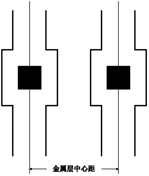
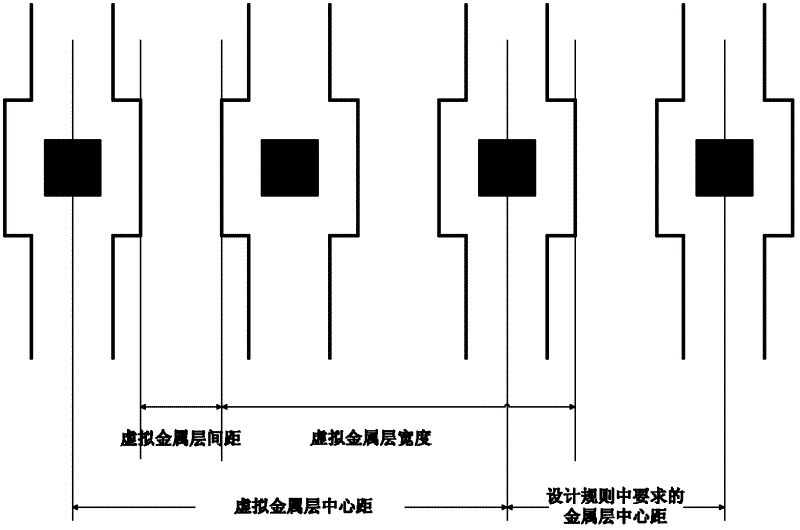
[0024] In order to clearly express the content of the invention, the layout design, design rules, metal layers, vias, connection vias, standard cell library and library model, comprehensive library model, physical library model, standard cell library design process, and metal layer center are firstly clarified. Definition of distance, grid point, wiring track, standard unit height, and standard unit minimum width.

[0025] Layout design:

[0026] In the manufacturing process of semiconductor integrated circuits, the planar design work of each real physical level in the complex manufacturing process, such as aluminum or copper interconnection lines, polycrystalline gates, etc., and graphics for impurity implantation regions, etc. The process of separation is called layout design, and the result of layout design is in the form of two-dimensional graphics, which are us...


PUM


Abstract

The invention discloses a method for designing a complementary data redundancy structure type CMOS (Complementary Metal Oxide Semiconductor) standard cell circuit physical library model. The method comprises the steps as follows: according to a cell library design flow, finishing the design of a cell circuit diagram and a layout with isolated input and output signals of a PMOS (P-channel Metal Oxide Semiconductor) network and an NMOS (N-channel Metal Oxide Semiconductor) network; virtually connecting the input and output ports of the PMOS network and the NMOS network in the circuit diagram and the layout respectively through auxiliary lines and auxiliary layers; designing a circuit diagram and a layout with functions of not distinguishing the input and output ports of the PMOS network and the NMOS network; and according to the method for designing the physical library model, extracting from the layout added with auxiliary connections to obtain the physical library model satisfying the EDA (Electronic Design Automation) tool format requirements, and setting special grid points and special wiring tracks in technology files at the same time. According to the method, the ultra-large-scale integrated circuit designed by adopting the complementary data redundancy structure type CMOS can be finished by using the semi-custom design based on the standard cell, so that the design efficiency of the circuit is improved.

Description

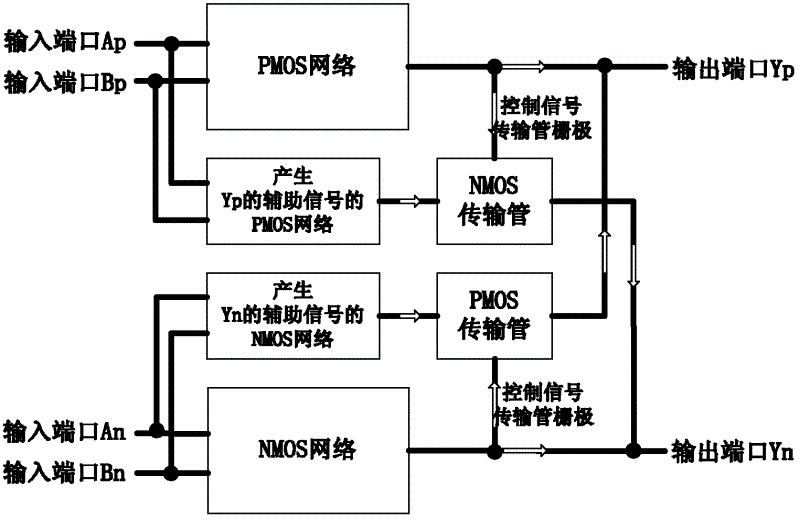
Technical field: [0001] The invention relates to the field of semiconductor integrated circuits, in particular to a method for designing a cell library physical library model of a complementary data redundant structural circuit. Background technique: [0002] The design method of the "Dual Data Stream" Spatial Redundancy circuit is to combine the PMOS (P-channel Metal Oxide Semiconductor) network and the NMOS (N-channel Metal Oxide Semiconductor) network in the CMOS (Complementary Metal Oxide Semiconductor) circuit. Semiconductor) network input and output signal isolation. The circuit designed by this method can effectively suppress the propagation of the transient pulse caused by the incident foreign particles into the reverse-biased diode junction of the CMOS circuit. With the deepening of research, there are many ways to realize the circuit, and the application range is more and more extensive. [0003] figure 1 A schematic diagram of the circuit structure of the comple...

Claims


Application Information

Patent Timeline
IPC IPC(8): G06F17/50
Inventor 赵德益王鹏李海松王忠芳卢红利岳红菊吴龙胜
Owner NO 771 INST OF NO 9 RES INST CHINA AEROSPACE SCI & TECH
Learn More