Production method for array substrate of active-matrix organic light-emitting display (OLED)

A technology for light-emitting displays and array substrates, applied in semiconductor/solid-state device manufacturing, electrical components, circuits, etc., can solve problems affecting display quality, electrode material fracture, etc., to improve display quality, reduce step difference, and reduce the probability of occurrence Effect

Active Publication Date: 2012-08-01
KUNSHAN NEW FLAT PANEL DISPLAY TECH CENT
View PDF6 Cites 11 Cited by
  • Summary
  • Abstract
  • Description
  • Claims
  • Application Information

AI Technical Summary

Problems solved by technology

At present, in the active matrix organic light-emitting display manufacturing process, usually after the formation of the transparent electrode layer and before the evaporation process starts, an array mask is used to form a protective film layer with a thickness of several microns to avoid the evaporation of the evaporation mask. Damage occurs during evaporation of the organic film layer, but if the film surface of the protective film produced has a large step difference, it is easy to cause the subsequent evaporation of the electrode material to break at the step, thereby affecting the display quality

Method used


Image

  • Production method for array substrate of active-matrix organic light-emitting display (OLED)
  • Production method for array substrate of active-matrix organic light-emitting display (OLED)
  • Production method for array substrate of active-matrix organic light-emitting display (OLED)

Examples


Embodiment Construction

[0034] The present invention will be further described below in conjunction with the accompanying drawings and embodiments.

[0035] During the manufacturing process of the AMOLED array substrate, a photolithography mask process is usually used to form a layer with a specific shape. These layers of specific shapes constitute the key devices and circuit structures of AMOLED.

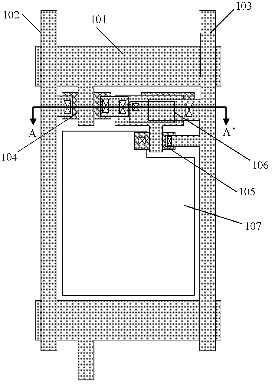
[0036] figure 1 It is a schematic diagram of a pixel structure of an active matrix organic light emitting display.

[0037] See figure 1 , the pixel structure of an active matrix organic light emitting display includes: a scanning line 101, a data line 102, a driving voltage line 103, a switching thin film transistor 104, a driving thin film transistor 105, a storage capacitor electrode 106 and a pixel display area 107.

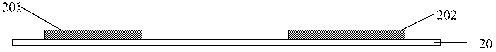
[0038] Figure 2 is figure 1 Schematic diagram of the fabrication process of each film layer at the A-A' section in the middle.

[0039] Such as Figure 2A As shown, firstly, a buf...


PUM

PropertyMeasurementUnit
thicknessaaaaaaaaaa

Abstract

The invention discloses a production method for an array substrate of an active-matrix organic light-emitting display (OLED). The production method comprises the following steps of: providing a substrate; forming a first semiconductor graph and a second semiconductor graph on the substrate; continuing to form a grid insulating layer and a first metal layer, and forming a grid by photo-etching; depositing an interlayer insulating layer, and forming four contact holes by means of etching; continuing to form a second metal layer, a source, a drain and a storage capacitor electrode; then continuing to form a passivation insulating layer and a transparent electrode layer; and finally forming a protecting film layer and an evaporation material layer on the whole surface, and exposing by a multi-grey-scale mask plate to form a stepped protecting film layer. In the production method for the array substrate of the OLED provided by the invention, the multi-grey-scale mask plate is used for exposing to form the stepped protecting film layer, thus effectively reducing the step difference of the protecting film layer and decreasing the occurrence probability of the poor display of the point defects of an AMOLED (active-matrix/organic light-emitting diode), and then improving the display quality of the AMOLED.

Description

technical field [0001] The invention relates to a method for manufacturing an array substrate, in particular to a method for manufacturing an array substrate of an active matrix organic light-emitting display. Background technique [0002] Organic light-emitting display (OLED) has the advantages of self-illumination, wide viewing angle, high contrast, thinness, and low power consumption. Next-generation flat-panel display technology after transistor liquid crystal display (TFT LCD). Generally, OLED displays have a stacked structure, using organic light-emitting compounds such as small molecule materials, polymers or other light-emitting materials as the organic light-emitting layer, which is placed between the cathode and the anode. According to different driving methods, OLED displays can be divided into active matrix type (Active Matrix) and passive matrix type. [0003] An active matrix organic light emitting display (hereinafter referred to as AMOLED) drives an organic...

Claims


Application Information

Patent Timeline
Patent Type & Authority Applications(China)
IPC IPC(8): H01L21/77
Inventor 高孝裕邱勇黄秀颀韩珍珍胡思明
Owner KUNSHAN NEW FLAT PANEL DISPLAY TECH CENT
Why Eureka
Try Eureka