Method for producing two layers of semiconductor devices with half empty structure

A semiconductor and semi-hollow technology, applied in semiconductor/solid-state device manufacturing, electrical components, circuits, etc., can solve problems such as increasing parasitic capacitance of semiconductor devices, limiting circuit response speed, increasing process complexity, etc., achieving simple process, The effect of increasing the degree of integration

Active Publication Date: 2012-08-01
SHANGHAI HUALI MICROELECTRONICS CORP
View PDF6 Cites 1 Cited by
  • Summary
  • Abstract
  • Description
  • Claims
  • Application Information

AI Technical Summary

Problems solved by technology

[0005] Chinese patent CN1610114A discloses a three-dimensional complementary metal-oxide-semiconductor device (CMOS) structure and its preparation method. It adopts low-temperature bonding and low-temperature lift-off technology, which can realize multi-layer stacking of CMOS and increase device integration density, but has the following defects : A layer of metal layer needs to be added between layers, and the upper and lower layers of devices are connected to it through through holes; this increases the complexity of the process
[0006] Chinese patent CN100440513C discloses a three-dimensional complementary metal-oxide-semiconductor (CMOS) device structure and its preparation method. It adopts low-temperature bonding and low-t

Method used


Image

  • Method for producing two layers of semiconductor devices with half empty structure
  • Method for producing two layers of semiconductor devices with half empty structure
  • Method for producing two layers of semiconductor devices with half empty structure

Examples


Embodiment Construction

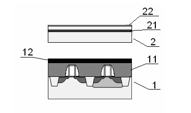
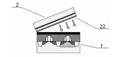
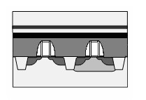
[0039] The invention provides a method for preparing a two-layer semiconductor device and a semiconductor device prepared by the method, Figure 1~Figure 11 A schematic flow diagram of the preparation of a two-layer semiconductor device in one embodiment of the present invention is given; below, with reference to the accompanying drawings, the present invention will be introduced and described in detail through specific embodiments, so as to better understand the content of the present invention, but it should be understood Yes, the following examples do not limit the scope of the present invention.

[0040]

[0041] In this embodiment, a planar CMOS FET structure is taken as an example, but various semiconductor devices may also be used.

[0042]

[0043] step 1

[0044] refer to figure 1 , the lower supporting sheet 1 has been patterned, and the supporting sheet 1 is selected from a bulk silicon wafer, and may also be an SOI silicon wafer, or other semiconductor wafers s...


PUM


Abstract

According to the invention, the methods of low-temperature bonding and low-temperature exfoliation are utilized to achieve the layer transfer of an upper semiconductor layer above a lower semiconductor device layer, then an upper semiconductor device is produced in the upper semiconductor layer, and finally, the processes for an upper contact hole and a lower contact hole are completed in one time to realize isolation in production of the upper and the lower layers of semiconductor devices. The method provided by the invention has the advantage of simple process. The integration level of the semiconductor devices is increased effectively. Additionally, a half empty isolation structure of an empty layer and the lower contact hole is produced between the upper and the lower layers of the semiconductor devices to effectively reduce the capacitance coupling effect between the upper and the lower layers of the semiconductor devices.

Description

technical field [0001] The invention relates to a method for preparing a semiconductor device, in particular to a method for preparing an upper and lower layer semiconductor device with a half-hole isolation structure. Background technique [0002] Due to its unique structure and a series of excellent properties, SOI (Silicon On Insulator) can realize the insulation isolation of components in integrated circuit manufacturing and eliminate the parasitic latch effect in bulk silicon CMOS; at the same time, CMOS / SOI circuits also have parasitic capacitance A series of advantages such as small size, high integration, fast speed, low power consumption, high working temperature (300°C), and radiation resistance. Therefore, SOI materials will be one of the main materials for thinner line (0.1μm) integrated circuits. It is expected that the above materials will be mainly used when the integration level reaches 1Gb and uses Φ300mm silicon wafers. In recent years, the rapid developme...

Claims


Application Information

Patent Timeline
IPC IPC(8): H01L21/8238H01L21/768
Inventor 黄晓橹
Owner SHANGHAI HUALI MICROELECTRONICS CORP
Why Eureka
Try Eureka