High-voltage withstanding device in bipolar low-voltage process and manufacturing method thereof

A manufacturing method and high-voltage-resistant technology, applied in semiconductor/solid-state device manufacturing, semiconductor devices, electrical components, etc., can solve problems such as worsening leakage problems, hot carrier injection, circuit function failure, etc.

Inactive Publication Date: 2012-08-01
HANGZHOU SILAN INTEGRATED CIRCUIT +1
View PDF6 Cites 6 Cited by
  • Summary
  • Abstract
  • Description
  • Claims
  • Application Information

AI Technical Summary

Problems solved by technology

The reliability failure of high-temperature operation is manifested in that when this type of circuit works at high temperature and high pressure, the high voltage is applied to the isolated PN junction with a large electric field strength, which will cause hot carrier injection, which will cause the leakage of the isolated PN junction to be too large, and at the same time, the chip internal Or the impact of external mobile ions will worsen the leakage problem and cause the circuit function to fail

Method used


Image

  • High-voltage withstanding device in bipolar low-voltage process and manufacturing method thereof
  • High-voltage withstanding device in bipolar low-voltage process and manufacturing method thereof
  • High-voltage withstanding device in bipolar low-voltage process and manufacturing method thereof

Examples


Embodiment Construction

[0028] In order to make the content of the present invention clearer and easier to understand, the content of the present invention will be further described below in conjunction with the accompanying drawings. Of course, the present invention is not limited to this specific embodiment, and general replacements known to those skilled in the art are also covered within the protection scope of the present invention.

[0029] Secondly, the present invention is described in detail by means of schematic diagrams. When describing the examples of the present invention in detail, for the convenience of explanation, the schematic diagrams are not partially enlarged according to the general scale, which should not be used as a limitation of the present invention.
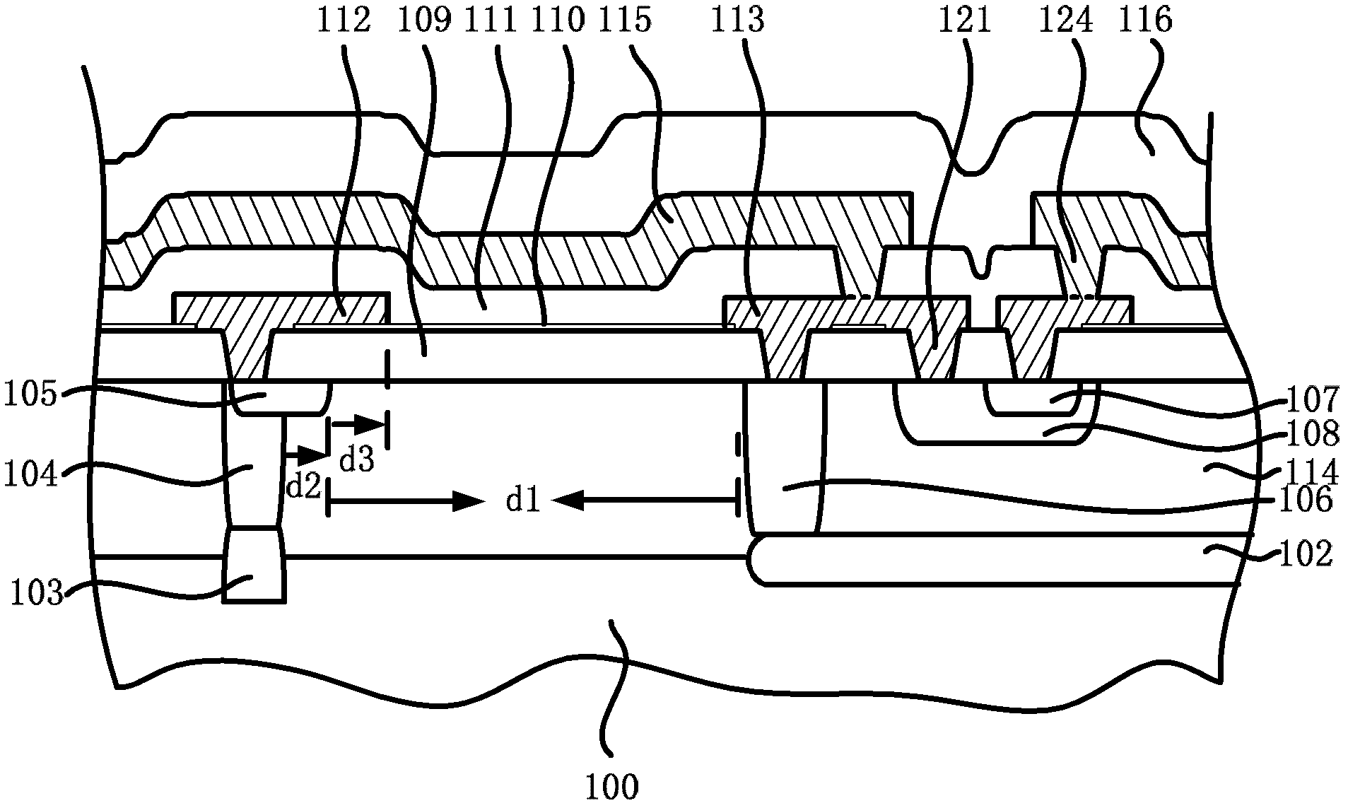
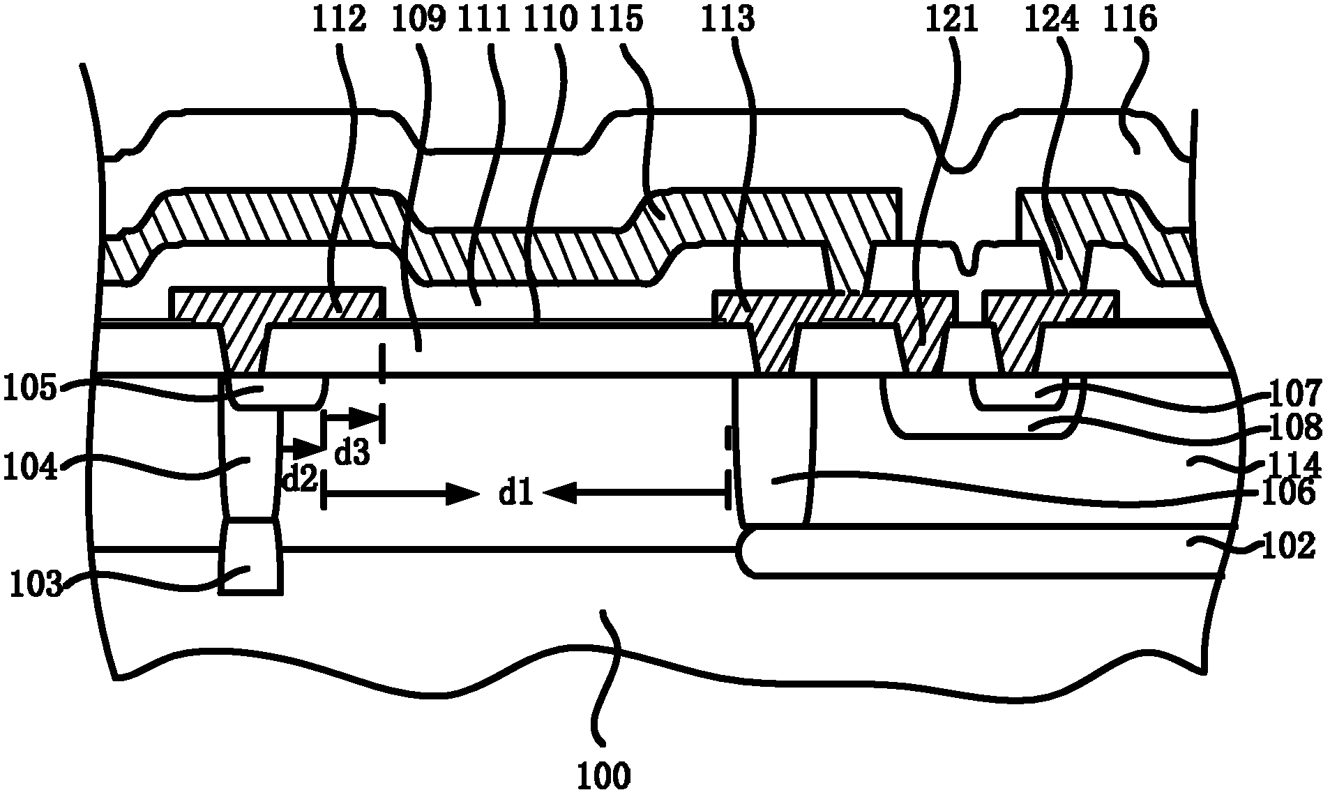
[0030] The core idea of ​​the present invention is to form a lightly doped region with a low doping concentration on the upper isolation region surrounding the collector region in the high-voltage resistant device in the Bipol...


PUM


Abstract

The invention provides a high-voltage withstanding device in a bipolar low-voltage process and a manufacturing method thereof. In the high-voltage withstanding device in the bipolar low-voltage process, a lightly doped region with low doping concentration is formed on an upper isolation region surrounding a current collection zone, the width of an earth-pole lead is more than that of the lightly doped zone, one side, facing the current collection zone, of the lightly doped region surpasses the upper isolation region by a certain width, one side, facing the current collection zone, of the earth-pole lead surpasses the lightly doped region by a certain width, so that the device in high-voltage work is prevented from a situation that a large amount of charges accumulate at an apex angle position of the upper isolation zone, the breakdown problem caused by charge accumulation is prevented, and thus, the performance of the device is increased. In addition, a silicon nitride layer on a first interlayer dielectric layer is combined with a passivation layer of a silicon-nitride-containing thin film layer, so that mobile ions can be effectively prevented from entering a strong electric field region in the high-voltage device structure to cause pollution, and thus, the high-temperature and high-voltage reliability of the high-voltage device can be guaranteed.

Description

technical field [0001] The invention relates to the technical field of semiconductor manufacturing, in particular to a high-voltage-resistant device in a Bipolar low-voltage process and a manufacturing method thereof. Background technique [0002] The classification of the traditional Bipolar (bipolar) process platform is generally formulated based on the maximum operating voltage that the standard NPN transistor manufactured by the process platform can withstand; the maximum operating voltage of the standard NPN transistor is from the collector area (C pole) to the emitter area ( The withstand voltage of E pole) (ie, CE withstand voltage) is determined. The CE withstand voltage is mainly determined by the epitaxial thickness and resistivity, and the base concentration and junction depth will also affect it; the epitaxial thickness determines the isolation rule and process, and the isolation rule and process The layout area is also determined; therefore, the Bipolar low-volt...

Claims


Application Information

Patent Timeline
Patent Type & Authority Applications(China)
IPC IPC(8): H01L29/70H01L29/06H01L29/36H01L21/328
Inventor 李小锋韩健张佼佼王铎
Owner HANGZHOU SILAN INTEGRATED CIRCUIT
Why Eureka
Try Eureka