Manufacturing method of low-temperature polycrystalline silicon (poly-Si) thin film transistor (TFT)

A thin-film transistor and low-temperature polysilicon technology, which is used in the manufacture of semiconductor/solid-state devices, electrical components, circuits, etc., can solve the problems of unevenness, disordered amorphous silicon film grains, and low electron mobility.

Active Publication Date: 2012-08-08
CENTURY DISPLAY (SHENZHEN) CO LTD
View PDF5 Cites 30 Cited by
  • Summary
  • Abstract
  • Description
  • Claims
  • Application Information

AI Technical Summary

Problems solved by technology

Since the amorphous silicon deposited by plasma-assisted chemical vapor deposition equipment contains 8-15% hydrogen content (hydrogen content), if excimer laser annealing is performed without dehydrogenation, the silicon film will instantly absorb huge excimer laser energy , and hydrogen explosion occurs in the excimer laser annealing area, thus causing the silicon film to easily fall off from the substrate (ablation), so it is necessary to dehydrogenate the PECVD silicon film before the excimer laser annealing, and the amorphou...

Method used


Image

  • Manufacturing method of low-temperature polycrystalline silicon (poly-Si) thin film transistor (TFT)
  • Manufacturing method of low-temperature polycrystalline silicon (poly-Si) thin film transistor (TFT)
  • Manufacturing method of low-temperature polycrystalline silicon (poly-Si) thin film transistor (TFT)

Examples


Embodiment Construction

[0027] In order to make the present invention more comprehensible, preferred embodiments are introduced in detail below. The preferred embodiments of the present invention are provided with corresponding reference numerals in the drawings.

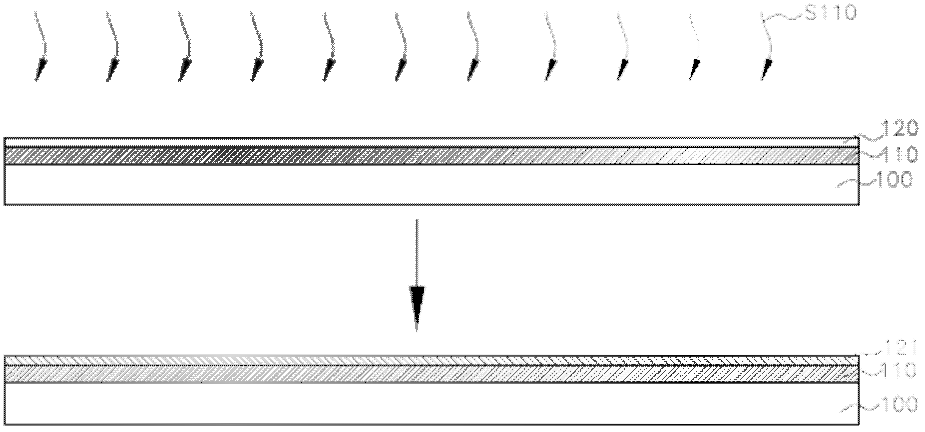
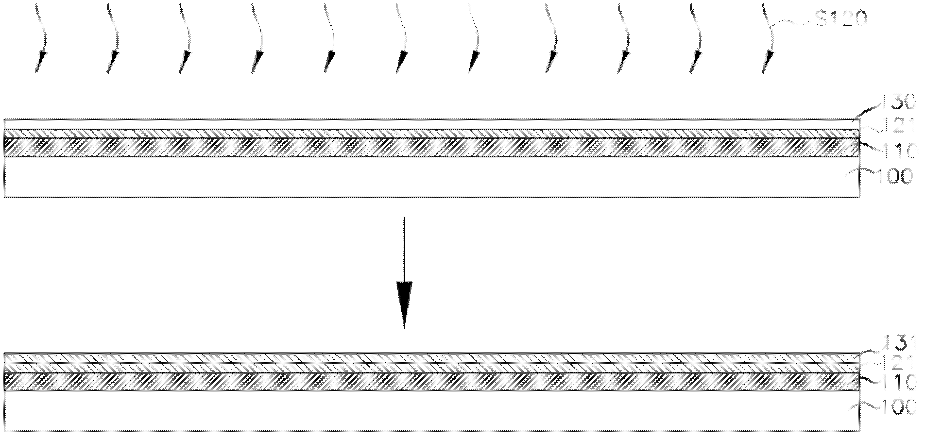
[0028] Figure 1 to Figure 11 It is a schematic diagram of a low-temperature polysilicon thin film transistor manufacturing method, please refer to Figure 1 to Figure 7 It is a schematic diagram of the method for forming a low-temperature polysilicon film of the present invention. A method for manufacturing a low-temperature polysilicon thin film transistor in this embodiment includes the following steps. First, a buffer layer 110 is formed on a substrate 100, wherein the method for forming the buffer layer 110 may be a low pressure chemical vapor deposition (low pressure CVD, LPCVD) process or a plasma enhanced chemical vapor deposition (plasma enhanced CVD, PECVD) process In more detail, the buffer layer 110 is, for example, a single l...


PUM


Abstract

The invention discloses a manufacturing method of a low-temperature polycrystalline silicon (poly-Si) thin film transistor (TFT). The method is characterized by: forming an amorphous silicon (a-Si) layer on a substrate; carrying out hydrogen relief treatment on the a-Si layer so that the a-Si layer becomes a microgranular; then, forming the a-Si layer which does not be performed with grain refining on the a-Si layer of the microgranular; and then carrying out the hydrogen relief treatment on the a-Si layer so that the a-Si layer becomes the microgranular; and continuously repeating so as to form the a-Si layer and carrying out the hydrogen relief treatment so as to form the a-Si layer with multilayer micromeritics; finally, carrying out excimer laser annealing (ELA) so that the a-Si layer with the multilayer micromeritics crystallizes into a poly-Si layer. After the poly-Si layer becomes the a-Si layer of the multilayer micromeritic through pretreatment, the ELA is performed so that the crystalline grain of the poly-Si layer becomes larger and a carrier mobility is high.

Description

【Technical field】 [0001] The invention relates to a manufacturing method of a low-temperature polysilicon thin-film transistor, in particular to a low-temperature polysilicon thin film which preprocesses an amorphous silicon layer to become a multi-layer microcrystalline amorphous silicon layer and then performs an excimer laser annealing process Transistor manufacturing method. 【Background technique】 [0002] With the development of high technology, video products, especially digital video or image devices have become common products in daily life. In these digital video or image devices, the display is an important component to display relevant information. Users can read information from the display, or further control the operation of the device. [0003] Thin-film transistors (TFT) can be applied to drive components of liquid crystal displays (LCDs for short), making LCDs the mainstream of straight flat-panel displays on desktops, as well as personal computers, game c...

Claims


Application Information

Patent Timeline
IPC IPC(8): H01L21/331H01L21/324
Inventor 许民庆吴钊鹏庄涂城余鸿志吴宏哲
Owner CENTURY DISPLAY (SHENZHEN) CO LTD
Why Eureka
Try Eureka