
Antenna housing for reducing minor lobe level by using artificial structure material
An artificial structure and radome technology, which is applied in the field of radome, can solve the problems of lowering the antenna, etc., and achieve the effect of simple manufacturing process, simple and novel design method, and light weight
- Summary
- Abstract
- Description
- Claims
- Application Information
AI Technical Summary
Problems solved by technology
Method used
Image

Examples
Embodiment Construction
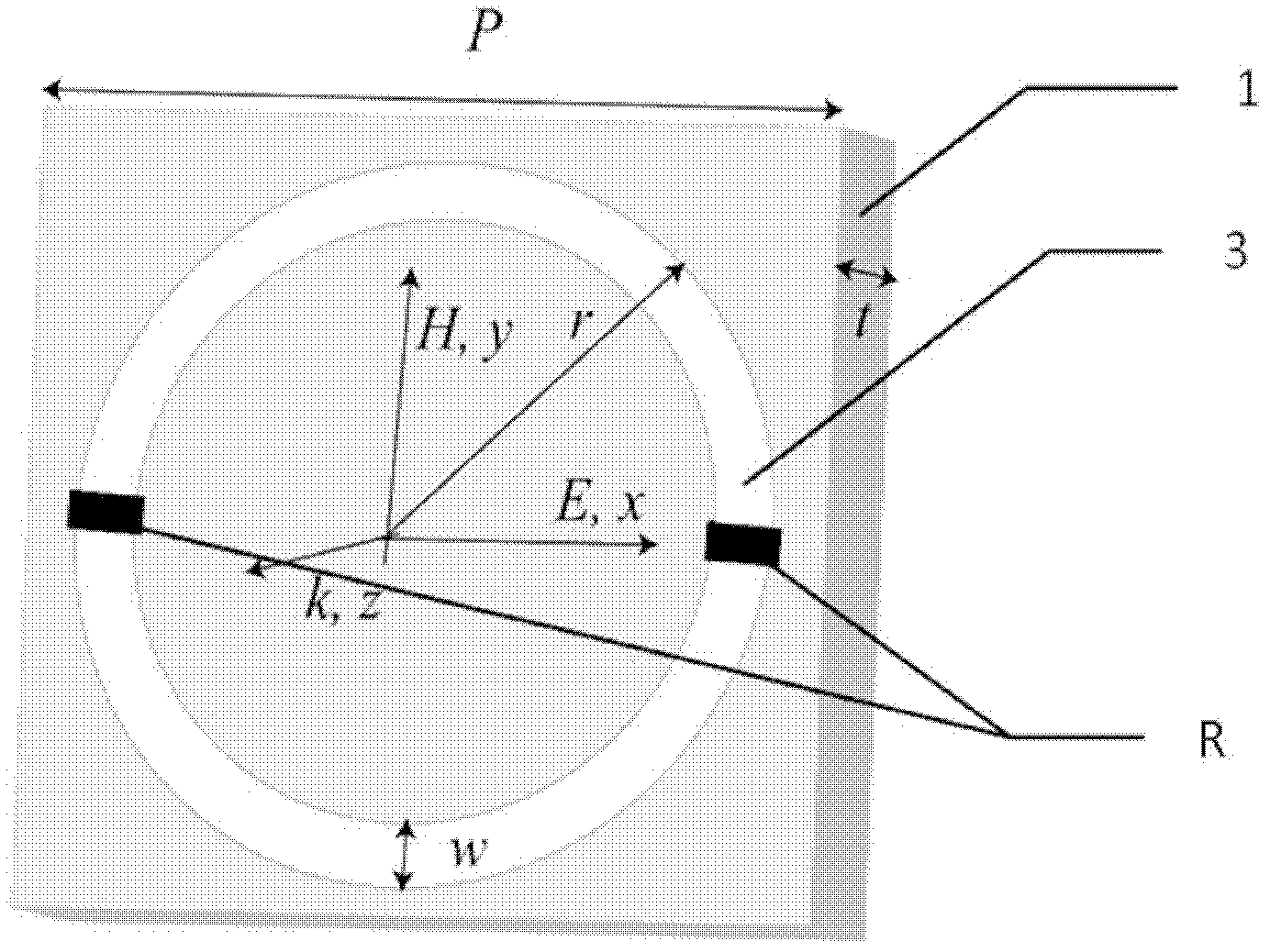
[0020] Such as figure 1 As shown, in order to make such a radome that uses artificial structural materials to reduce the sidelobe level, a single-sided copper-clad microwave dielectric plate printed with annular slits is used, and two chip resistors R are added symmetrically along the transverse direction. In the xyz coordinate system, k is the direction of the incident wave along the z axis, E is the direction of the electric field along the x axis, and H is the direction of the magnetic field along the y axis. Where P represents the unit period, r represents the radius of the outer ring, w represents the width of the annular gap, t represents the thickness of the dielectric plate, and R represents the chip resistance.
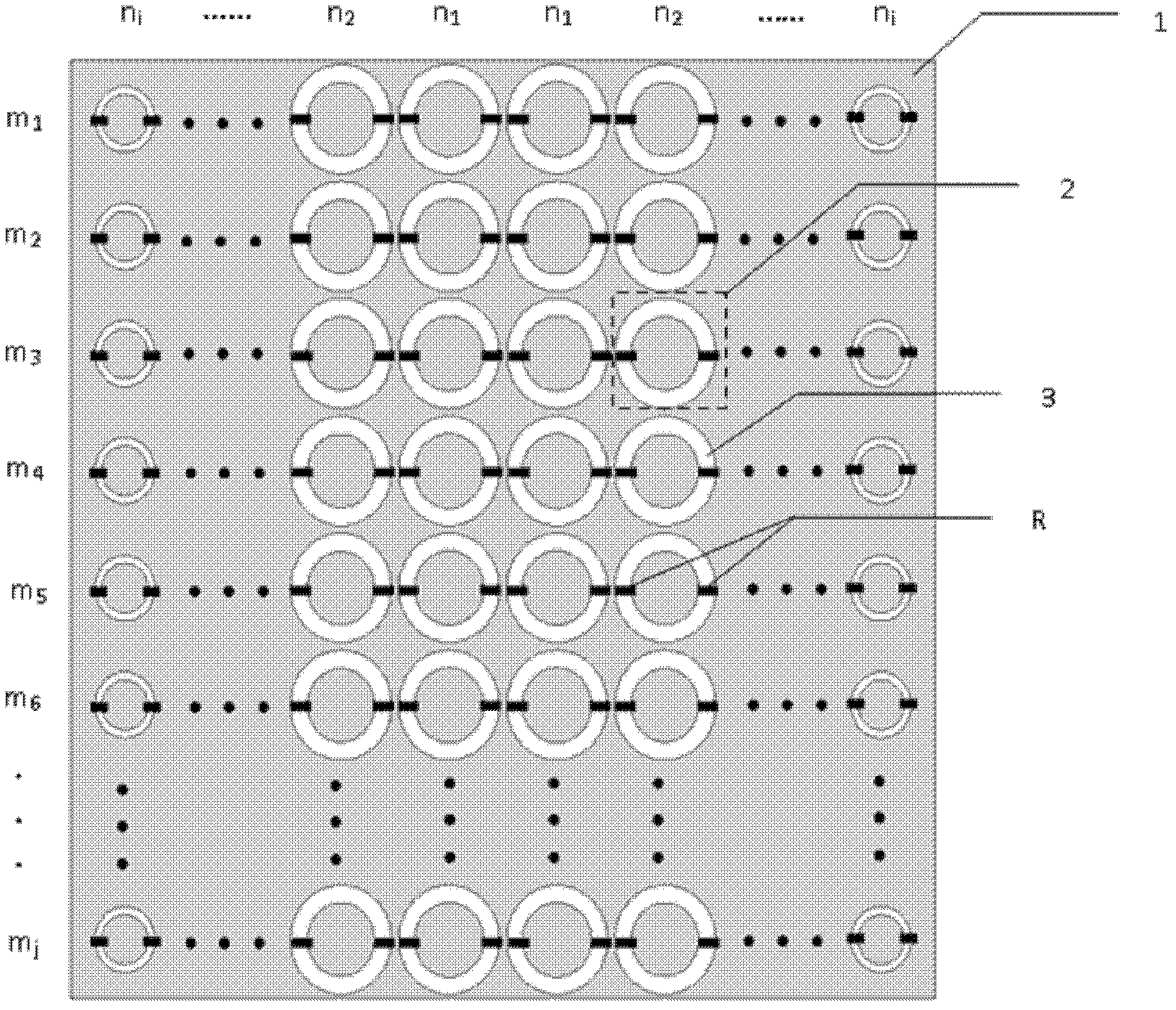
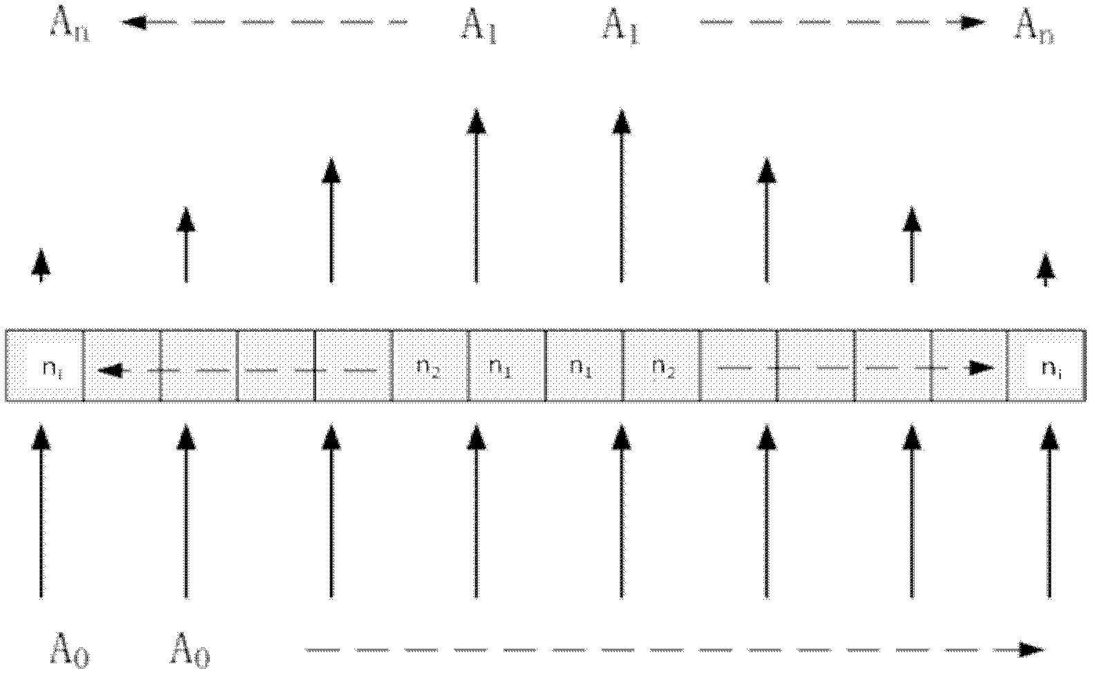
[0021] figure 2 A schematic diagram of the overall structure of the radome designed for the invention. Print 2n on the single-sided copper-clad microwave dielectric board 1, respectively i Column×m j Row ring-shaped gap structure 2, of which 2n i Columns of ann...
PUM
 Abstract
Description
Claims
Application Information