Computing method for diffraction field of double-absorbing-layer alternating phase shift contact hole mask

A mode diffraction field and double-absorbing layer technology, which is applied in the field of calculation of the diffraction field of the double-absorbing layer alternating phase-shift contact hole mask, can solve the problems of poor convergence and the inability to calculate the double-absorbing layer alternating phase-shift contact hole mask diffraction, etc.

Active Publication Date: 2012-08-15
BEIJING INSTITUTE OF TECHNOLOGYGY
View PDF5 Cites 2 Cited by
  • Summary
  • Abstract
  • Description
  • Claims
  • Application Information

AI Technical Summary

Problems solved by technology

However, this method has the following disadvantages. It can only analyze multi-layer two-dimensional gratings with the same period; this method analyzes the diffraction characteristics of dielectric gratings, and the convergence is poor; at the same time, this method only analyzes the diffraction of one layer of two-dimensional gratings. In the alternating phase shift contact hole mask, the mask has three grating layers, and the period of the etched area in the glass substrate in two orthogonal directions (x, y) is twice the corresponding period of the mask absorbing layer, The periods in the two orthogonal directions are different, and the phase-shifting region of the substrate exhibits a crossed grating characteristic
Therefore, the above method cannot be used to calculate the diffraction of the double absorbing layer alternating phase shift contact hole mask

Method used


Image

  • Computing method for diffraction field of double-absorbing-layer alternating phase shift contact hole mask
  • Computing method for diffraction field of double-absorbing-layer alternating phase shift contact hole mask
  • Computing method for diffraction field of double-absorbing-layer alternating phase shift contact hole mask

Examples


example 1

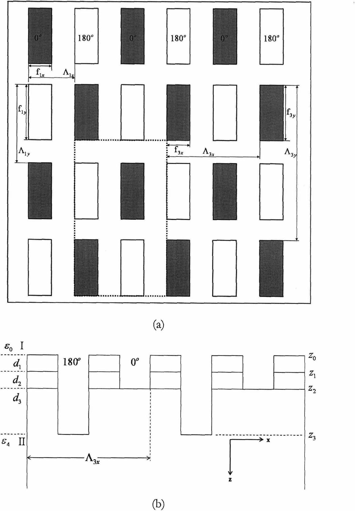
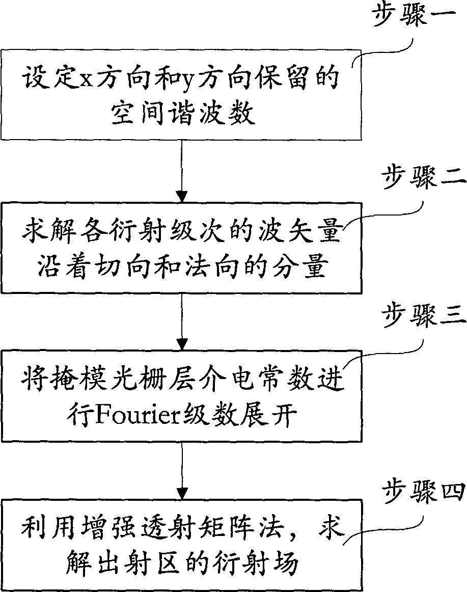
[0170] Here the TE conical incidence (θ=10°, When λ=193nm), the diffraction efficiencies of (0,0), (0,2), (1,1), (2,0) orders when different mask line widths (wafer scale). The refractive index, extinction coefficient and thickness of CrO are 1.965, 1.201 and 18nm respectively. The refractive index, extinction coefficient and thickness of CrO are 1.477, 1.762 and 55nm respectively. The duty cycle is 0.6.

[0171] Figure 16 Cone incident for TE polarized light (θ=10°, Diffraction efficiency of (0,0), (0,2), (1,1), (2,0) diffraction orders when λ=193nm) double absorption layer (CrO / Cr) alternating phase shift contact hole mask Graph as a function of feature size (wafer scale, nm). (a) The relationship diagram of the diffraction efficiency of (0,0) order light with the change of line width, (b) the relationship diagram of the diffraction efficiency of (0,2) order light with the change of line width, (c) (1,1) The relationship diagram of the diffraction efficiency of order...


PUM


Abstract

The invention provides a computing method for a diffraction field of a double-absorbing-layer alternating phase shift contact hole mask. According to the method, diffraction of the double-absorbing-layer alternating phase shift contact hole mask in photo-etching can be quickly computed. The computing method specifically comprises the following steps of: 1, setting harmonic number reserved in the x direction and setting harmonic number reserved in the y direction; 2, solving components of wave vector of each diffraction order in the tangential direction and the normal direction according to a Floquet condition; 3, performing Fourier series expansion on dielectric constant of a two-dimensional grating on each layer and a reciprocal of the dielectric constant; and 4, solving the diffraction field of an emission region by using an enhanced transmission matrix method. In two orthogonal directions, the Fourier series expansion is performed by selecting the minimum common multiple of cycles of three grating layers in the corresponding orthogonal direction, so that the diffraction of a plurality of layers of two-dimensional mask gratings with different cycles in the two orthogonal directions can be analyzed, and meanwhile, the diffraction field of the double-absorbing-layer alternating phase shift contact hole mask can be quickly solved.

Description

technical field [0001] The invention relates to a method for calculating the diffraction field of a double-absorbing layer alternating phase-shift contact hole mask, and belongs to the technical field of lithographic resolution enhancement. Background technique [0002] The rapid development of the semiconductor industry is mainly due to the progress of micro-processing technology in microelectronics technology, and photolithography technology is one of the most critical manufacturing technologies in chip preparation. Due to the continuous innovation of optical lithography technology, it has repeatedly broken through the expected optical exposure limit, making it the mainstream technology of current exposure. [0003] The lithography system is mainly divided into four parts: illumination system (light source), mask, projection system and wafer. The light incident on the mask is diffracted, and the diffracted light enters the projection system and forms an interference image...

Claims


Application Information

Patent Timeline
Patent Type & Authority Applications(China)
IPC IPC(8): G03F1/26G03F1/30
Inventor 李艳秋杨亮
Owner BEIJING INSTITUTE OF TECHNOLOGYGY
Why Eureka
Try Eureka