Manufacturing method of surface conduction electron emission source with uniform and controllable nano gaps

A nano-gap and electron-conducting technology, which is applied in the manufacture of discharge tubes/lamps, electrode system manufacturing, circuits, etc., can solve the difficulty of controlling the spacing and uniformity of nano-gap, the complicated process of making electron emission sources, and the failure of electron emission sources, etc. problem, achieve the effect of improving emission efficiency and uniformity, low cost, and avoiding pollution

Active Publication Date: 2012-08-15
FUZHOU UNIV
View PDF3 Cites 12 Cited by
  • Summary
  • Abstract
  • Description
  • Claims
  • Application Information

AI Technical Summary

Problems solved by technology

There are two main problems in the manufacturing process of traditional SED electron emission sources: (1) Regardless of using Joule heat or special laser beam technology, the manufacturing process of electron emission sources is complicated, and the spacing and uniformity of nano-gap are difficult to control; (2) A voltage is applied between the two electrodes to burn the nano-gap. Due to the unevenness of the electrodes, local high-resistance substances are generated, resulting in the failure of local electron emission sources.
[0005] Aiming at the complex manufacturing process of the traditional SED electron emission source, it is easy to cause partial failure of the electron emission source, etc., the present invention proposes a new manufacturing method of the surface conduction electron emission source

Method used


Image

  • Manufacturing method of surface conduction electron emission source with uniform and controllable nano gaps
  • Manufacturing method of surface conduction electron emission source with uniform and controllable nano gaps
  • Manufacturing method of surface conduction electron emission source with uniform and controllable nano gaps

Examples


specific Embodiment

[0041] A specific embodiment comprises the following steps:

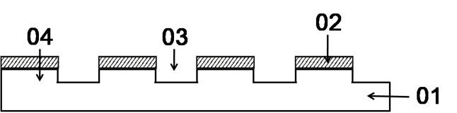
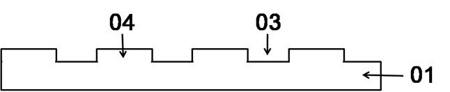
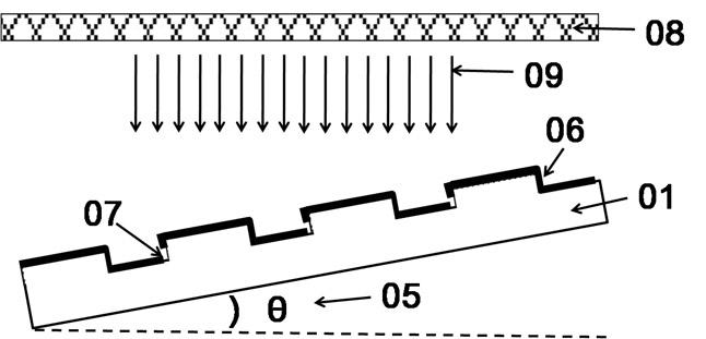
[0042] (S11) Fabrication of column pattern arrays:

[0043] Select a glass substrate of the required size for scribing, place the glass substrate in a cleaning solution with a volume ratio of Win-10: DI water = 3: 97, use an ultrasonic machine with a frequency of 32KHz to clean for 15 minutes, and spray for 2 minutes. Then place it in the cleaning solution with a volume ratio of Win-41: DI water = 5: 95, use an ultrasonic machine with a frequency of 40KHz to clean for 10 minutes, spray and rinse with circulating tap water for 2 minutes, and then use an ultrasonic machine with a frequency of 28KHz to clean it in DI Rinse in water for 10 minutes, blow dry with a nitrogen gun, and place in a clean oven at 50°C for at least 30 minutes for later use.

[0044] On the clean glass substrate 01, a layer of photoresist RZJ-304 was evenly coated by screen printing process, baked at 110°C for 20 minutes, and then exposed-deve...


PUM

PropertyMeasurementUnit
thicknessaaaaaaaaaa
heightaaaaaaaaaa

Abstract

The invention discloses a manufacturing method of a surface conduction electron emission source with uniform and controllable nano gaps. The manufacturing method comprises the following concrete steps of: firstly, preparing a columnar pattern array with height ranging from 10 nanometers to hundreds of nanometers and rectangular, triangular or trapezoidal vertical cross section on a flat insulation substrate; then depositing an SED (surface-conduction electron-emitter display) electron-emitting source film layer with the thickness ranging from 10 nanometers to 500 nanometers toward an inclined direction on the flat insulation substrate prepared with the columnar pattern; directly producing a gap with the width ranging from a few nanometers to dozens of nanometers or by virtue of follow-up dry etching or wet etching as no film or extremely thin film is deposited on the part blocked by the columnar pattern; and finally manufacturing an SED electron emission electrode array on the substrate. The manufacturing process of the SED electron emission source is simple, and nano gaps which realize electron emission are uniform and controllable.

Description

technical field [0001] The invention relates to the technical field of surface conduction field emission flat panel display, in particular to a method for manufacturing a surface conduction electron emission source with uniform and controllable nano-gap. Background technique [0002] Field Emission Display (Field Emission Display, FED) is a fully solidified active light-emitting flat panel display technology. FED has the advantages of small size, light weight, and low power consumption. In addition, the response time of FED is at the microsecond level, and the operating temperature range is -45~+85°C, which has very obvious advantages. Among them, Surface-conduction Electron-emitter Display (SED) has attracted extensive attention from the industry due to its high contrast ratio, low power consumption, and fast screen response speed. [0003] The key technology of SED is the manufacture of electron emission source. SED electron emission source is usually a very thin conducti...

Claims


Application Information

Patent Timeline
Patent Type & Authority Applications(China)
IPC IPC(8): H01J9/02
Inventor 周雄图郭太良张永爱叶芸林志贤姚剑敏曾祥耀
Owner FUZHOU UNIV
Why Eureka
Try Eureka