Terminal structure of channel power metal oxide semiconductor (MOS) device and manufacture method of terminal structure

A technology of MOS device and terminal structure, applied in semiconductor/solid-state device manufacturing, semiconductor devices, electrical components, etc., can solve problems such as being susceptible to external influences and adverse device stability, and achieve chip cost and device reliability improvement and savings. The effect of mask plate times and protection breakdown voltage

Inactive Publication Date: 2012-08-15
HARBIN ENG UNIV
View PDF9 Cites 7 Cited by
  • Summary
  • Abstract
  • Description
  • Claims
  • Application Information

AI Technical Summary

Problems solved by technology

Its characteristics are: the terminal is composed of a series of deep grooves, and the polysilicon electrode is suspended in the terminal, so the P-region in the suspended electrode is easily affected by the outside world, which is not conducive to the stability of the device

Method used


Image

  • Terminal structure of channel power metal oxide semiconductor (MOS) device and manufacture method of terminal structure
  • Terminal structure of channel power metal oxide semiconductor (MOS) device and manufacture method of terminal structure
  • Terminal structure of channel power metal oxide semiconductor (MOS) device and manufacture method of terminal structure

Examples


Embodiment Construction

[0023] The present invention is described below in conjunction with accompanying drawing.

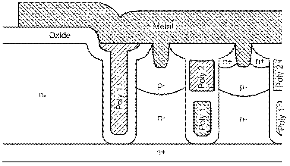
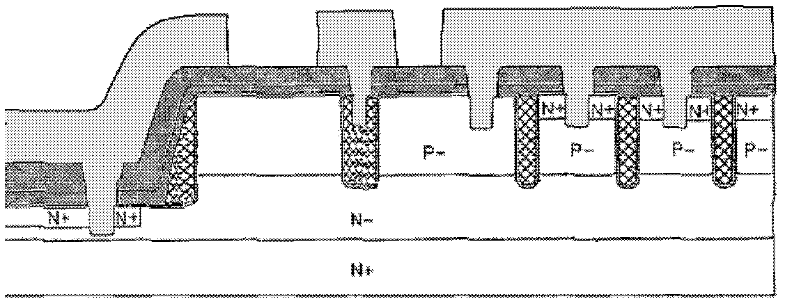
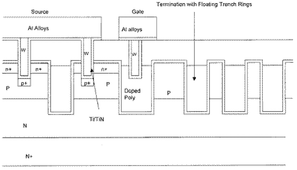
[0024] 1. In the terminal structure of the split gate trench power MOS device, the gate electrode lead-out structure and the corresponding lower split gate structure are produced under the same process conditions as the cells in the same device, as shown in the schematic diagram of the process steps in Figure 5 .

[0025] 2. In the process steps shown in Figure 5, the silicon nitride mask 1 is used to form a spacer oxide (Spacer Oxide) structure to etch out the trench gate structure, and it can also be used as the source electrode N+ ion implantation with the gate electrode lead-out part mask plate.

[0026] 3. Simulation curve of the breakdown characteristics of the split-gate trench MOSFET device. The breakdown voltage of the split-gate device is 35V (defined when the reverse drain-source current reaches 1×10 -12 device breakdown at A / μm).

[0027] 4. The internal current and poten...


PUM


Abstract

The invention provides a terminal structure of a channel power metal oxide semiconductor (MOS) device and a manufacture method of the terminal structure. The terminal structure comprises a grid electrode lead-out electrode (101), wherein a suspension polycrystalline silicon electrode (102) is arranged under the grid electrode lead-out electrode (101) and is positioned inside a thick oxidation layer (103), a grid electrode connecting metal (104) is arranged above the grid electrode lead-out electrode (101), a source electrode (105) of a device active region is arranged on the top of a cell structure, a drift region (106) adopts N type doping, a drain electrode (107) adopts N type heavy doping, and a combined structure of the grid electrode lead-out electrode (101), a grid electrode lower part suspension polycrystalline silicon electrode (102) and the thick oxidation layer (103) realizes the effect of a device terminal and is formed in the same mask and the same process. The ultra-low conducting resistance of the device is ensured, the breakdown voltage and the parasitic capacitance of the device cannot be influenced, the process manufacture flow process is optimized, and meanwhile, the manufacture cost of the device is reduced.

Description

technical field [0001] The invention relates to an electronic component, and the invention also relates to a preparation method of the electronic component. Specifically, it relates to a terminal structure of a trench power MOS device and a manufacturing method thereof. Background technique [0002] In the 1990s, the main research direction of the development of Power Trench MOSFET and industrialization technology was to minimize the forward conduction resistance (Ron) of low-voltage power devices. Today, the structure of power trench MOS devices is suitable for most power MOSFET applications, and the characteristics of the devices are constantly approaching the one-dimensional limit of silicon materials (expressing the characteristic on-resistance in the drift region of the device and the breakdown in the off-state Theoretical relationship of voltage). The proposal of REduced SURface Field (RESURF) technology can make power trench MOS devices with a breakdown voltage of 6...

Claims


Application Information

Patent Timeline
Patent Type & Authority Applications(China)
IPC IPC(8): H01L29/40H01L29/78H01L21/28H01L21/336
CPCH01L29/7813H01L29/407H01L29/42372H01L29/66734H01L29/7811
Inventor 王颖胡海帆焦文利曹菲
Owner HARBIN ENG UNIV
Why Eureka
Try Eureka