Atomizing jet device for cleaning

A technology of spraying device and shell, which is applied to spraying device, liquid spraying device, chemical instrument and method, etc., can solve the problems of low utilization rate of cleaning liquid and deionized water, damage of chip surface pattern, etc., and achieves simple structure and integrated High temperature and water saving effect

Active Publication Date: 2012-08-22
BEIJING NAURA MICROELECTRONICS EQUIP CO LTD
View PDF6 Cites 10 Cited by
  • Summary
  • Abstract
  • Description
  • Claims
  • Application Information

AI Technical Summary

Problems solved by technology

[0007] The technical problem to be solved by the present invention is to provide a cleaning atomization injection device with a simple structure that can spray ultra-fine atomized droplets, so as to overcome the simple atomization mechanism to generate large-size droplets or jet streams, and to 65 nanometers and The chip surface pattern of the following process causes serious damage, low utilization rate of cleaning solution and deionized water, etc.

Method used


Image

  • Atomizing jet device for cleaning
  • Atomizing jet device for cleaning
  • Atomizing jet device for cleaning

Examples


Embodiment Construction

[0028] The specific implementation manners of the present invention will be further described in detail below in conjunction with the accompanying drawings and embodiments. The following examples are used to illustrate the present invention, but are not intended to limit the scope of the present invention.

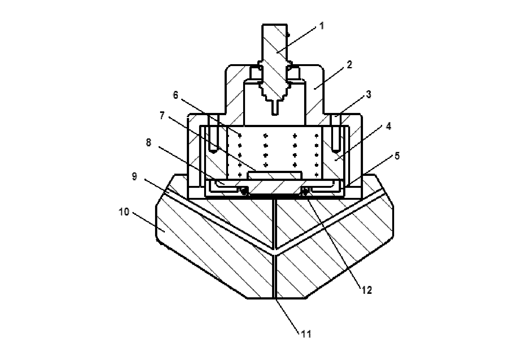
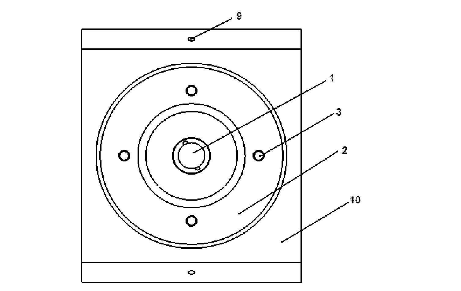
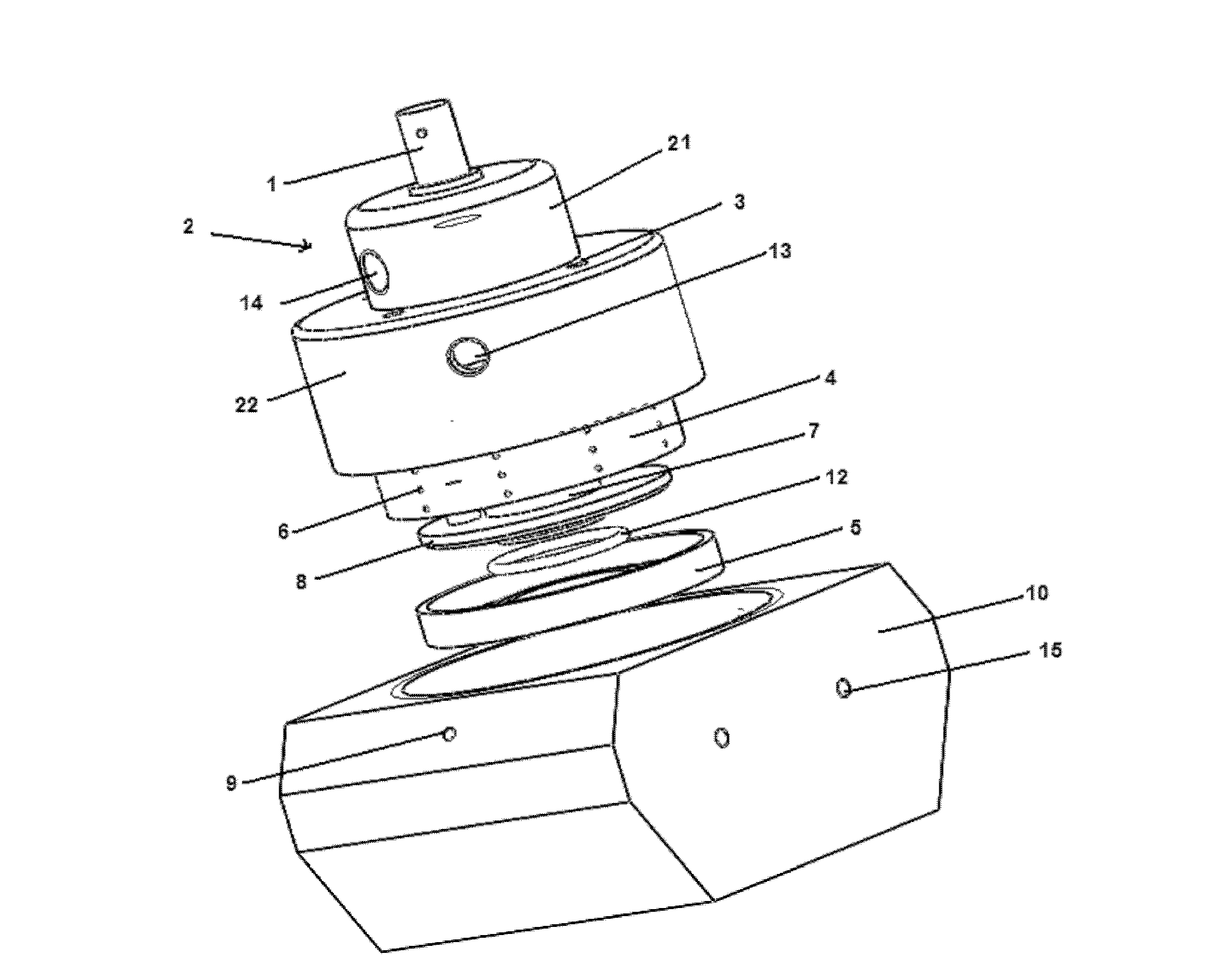
[0029] like Figure 1-5 As shown, the cleaning atomizing spraying device of the present invention includes: an upper casing 2 and a lower casing 10 connected together by threads or other connections, the upper casing 2 is made of PVDF or other high corrosion resistance and better strength Made of non-metallic materials. The upper shell 2 is a second-stage cylindrical shape, including a first-stage shell 21 and a second-stage shell 22, the cross-sectional area of ​​the first-stage shell 21 is smaller than the cross-sectional area of ​​the second-stage shell 22; The first-stage housing 21 is provided with a cable connector 1 that can be connected to a power amplifier (not ...


PUM


Abstract

The invention relates to the technical field of semiconductor chips, in particular to an atomizing jet device for cleaning, which comprises an upper casing and a lower casing connected with the upper casing. The upper casing is in the shape of a two-step cylinder including a first-step casing and a second-step casing, the cross section area of the first-step casing is smaller than that of the second-step casing, the first-step casing is provided with a cable joint capable of being connected with a power amplifier, and an energy transducer is arranged in the second-step casing. Vent holes are arranged on two side walls of the lower casing, an atomizing jet through hole is arranged at the center of the lower casing, and the vent holes are communicated with the atomizing jet through hole and form included angles with the same. The atomizing jet device for cleaning is simple in structure and high in integration degree, is capable of jetting ultra-micro-atomized liquid drops effectively and effectively cleaning the chips on the premise of protecting surface patterns of the chips while saving water resources to the utmost extent.

Description

technical field [0001] The invention relates to the technical field of semiconductor wafer technology, in particular to a cleaning atomization injection device. Background technique [0002] There are hundreds of cleaning processes in the manufacturing process of integrated circuits. In order to ensure the cleanliness of the surface of the wafer material, the cleaning process accounts for 30% of the entire manufacturing process. Wherein, the wafer refers to a silicon wafer with a pure silicon substrate and a silicon wafer with a copper interconnection structure. According to statistics, each silicon substrate chip with a diameter of 200 mm needs to consume 5 tons of high-purity deionized water in the entire manufacturing process, plus the cost of other various consumables in cleaning, it will be a very high figure. [0003] Further statistics show that more than 50% of the losses in the manufacturing of semiconductor devices are caused by surface contamination and incomplet...

Claims


Application Information

Patent Timeline
Patent Type & Authority Applications(China)
IPC IPC(8): B08B3/02B05B17/04
Inventor 刘效岩吴仪初国超刘海晓
Owner BEIJING NAURA MICROELECTRONICS EQUIP CO LTD
Why Eureka
Try Eureka