

Preparation method of FinFET (Fin Field Effect Transistor) in large-scale integration circuit
一种干法刻蚀、氮化硅的技术,应用在电路、电气元件、半导体/固态器件制造等方向,能够解决栅条宽度不能自对准形成、没有形成三栅结构等问题,达到避免栅材料残留、刻蚀量小、避免电学等效厚度增加的效果
- Summary
- Abstract
- Description
- Claims
- Application Information
AI Technical Summary
Problems solved by technology
Method used
Image

Examples
Embodiment Construction
[0041] The present invention can be implemented through the following specific examples, but is not limited to the range of process parameters mentioned in the following examples, and similar inventive spirits should also belong to the extension of the present invention.
[0042] Prepare FinFET devices according to the following steps:
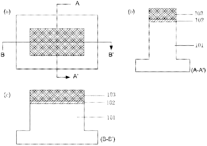
[0043] 1. On the bulk silicon substrate 101 of (100) or (110) crystalline direction, grow silicon dioxide and deposit silicon nitride as the hard mask of etching for the first time, wherein the thickness of silicon dioxide layer 102 is 50 angstroms ~200 angstroms, and the thickness of the silicon nitride layer 103 is 70 ~500 angstroms.
[0044] 2. Transfer the pattern of the active region to the silicon nitride layer 103 by using the first photolithography mask, and use the photoresist as a mask to etch the silicon nitride, and stop on the silicon dioxide layer 102 .
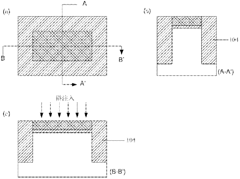
[0045] 3. Remove the photoresist, use silicon nitride as a hard mask to dr...
PUM
| Property | Measurement | Unit |
|---|---|---|
| depth | aaaaa | aaaaa |
Abstract
Description
Claims
Application Information