Three-dimensional array type back grid type Si-NWFET (Nano Wire Field Effect Transistor) manufacturing method based on SOI (Silicon On Insulator)

A technology of three-dimensional array and manufacturing method, applied in semiconductor/solid-state device manufacturing, electrical components, circuits, etc., can solve the problems of large interface state, inconvenience, unsuitable gate oxide layer, etc., and achieve increased current drive capability and increased isolation Effects, effects that facilitate the control of gate profile and device electrical properties

Active Publication Date: 2012-08-22
SHANGHAI HUALI MICROELECTRONICS CORP
View PDF5 Cites 5 Cited by
  • Summary
  • Abstract
  • Description
  • Claims
  • Application Information

AI Technical Summary

Problems solved by technology

[0009] This method can realize the vertically stacked silicon nanowire field effect transistor structure, but there is a disadvantage: when the silicon germanium layer is oxidized, the germanium will be concentrated to the surface of the silicon layer, and the SiO2 will be removed. 2 Finally, the Si-NW surface is coated with a layer of concentrated silicon-germanium alloy
Since germanium dioxide is soluble in water, the subsequent process faces great inconvenience. In addition, the dielectric constant of germanium dioxide is smaller than that of silicon dioxide, and the interface state between germanium dioxide and silicon is relatively large, so it is not suitable as the gate oxide layer of MOSFET.

Method used


Image

  • Three-dimensional array type back grid type Si-NWFET (Nano Wire Field Effect Transistor) manufacturing method based on SOI (Silicon On Insulator)
  • Three-dimensional array type back grid type Si-NWFET (Nano Wire Field Effect Transistor) manufacturing method based on SOI (Silicon On Insulator)
  • Three-dimensional array type back grid type Si-NWFET (Nano Wire Field Effect Transistor) manufacturing method based on SOI (Silicon On Insulator)

Examples


Embodiment Construction

[0056] In order to make the above objects, features and advantages of the present invention more comprehensible, specific implementations of the present invention will be described in detail below in conjunction with the accompanying drawings.

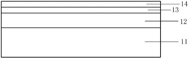
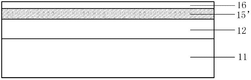
[0057] First, please refer to Figure 19 , in order to describe this embodiment more clearly, define the length direction of the fin-shaped active region or the silicon nanowire formed subsequently as the XX' direction, the XX' direction runs through the gate and the source and drain regions, and is perpendicular to the X-X' direction. X' direction is Y-Y' direction. Combine below Figures 1 to 19 Describe in detail the method for fabricating an SOI-based three-dimensional array Si-NWFET according to an embodiment of the present invention, specifically including:

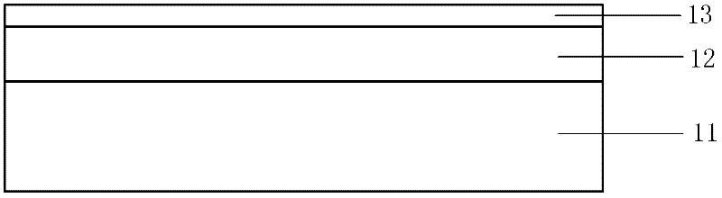
[0058] Please refer to figure 1 , provide SOI substrate, the bottom layer of SOI substrate is the silicon liner layer 11 for providing mechanical support, upwards are ins...


PUM

PropertyMeasurementUnit
diameteraaaaaaaaaa

Abstract

The invention provides a three-dimensional array type back grid type Si-NWFET (Nano Wire Field Effect Transistor) manufacturing method based on an SOI (Silicon On Insulator). The manufacturing method comprises the following steps of: alternatively depositing a silicon layer and a germanium-silicon layer on the SOI to form a fin-shaped active region, and forming a silicon nano wire in the fin-shaped active region, wherein the silicon nano wire is a three-dimensional array type; then, forming an isolating medium layer between source drain regions; forming a grid electrode oxidization layer on the surface of the silicon nano wire; and finally, forming a grid electrode on an SOI substrate in the fin-shaped active region. Due to the presence of an insulator layer in the SOI, the isolation effect between the grid electrode and the SOI substrate is effectively increased; a process for forming the grid electrode oxidization layer on the silicon nano wire is independently carried out so that the conventional grid electrode oxidization layer is adopted; and the grid electrode is formed after ions are injected into the source drain regions, namely a back grid electrode process is adopted, so that the preparation method is good for controlling an outline of the grid electrode and an electrical property of a device. Furthermore, a silicon nano wire field effect transistor structure is designed by a three-dimensional array type back grid type silicon nano wire structure; and the quantity of nano wires is increased and the current driving capability of the device can be increased.

Description

technical field [0001] The invention relates to the field of integrated circuit manufacturing, in particular to an SOI-based three-dimensional array gate-back Si-NWFET manufacturing method. Background technique [0002] It has always been the goal pursued by the development of microelectronics industry to increase the working speed and integration of chips and reduce the power consumption density of chips by reducing the size of transistors. In the past forty years, the development of microelectronics industry has been following Moore's Law. At present, the physical gate length of field effect transistors is close to 20nm, and the gate dielectric is only a few layers of oxygen atoms thick. It is difficult to improve performance by reducing the size of traditional field effect transistors, mainly because of the short Channeling and gate leakage destroy the switching performance of transistors. [0003] Nanowire Field Effect Transistor (NWFET, Nano-Wire MOSFET) is expected t...

Claims


Application Information

Patent Timeline
Patent Type & Authority Applications(China)
IPC IPC(8): H01L21/762H01L21/28H01L21/02H01L21/336
Inventor 黄晓橹
Owner SHANGHAI HUALI MICROELECTRONICS CORP
Why Eureka
Try Eureka