Method for directly writing organic semiconductor laser by ultraviolet laser interferometry etching

An organic semiconductor and ultraviolet laser technology, applied in semiconductor devices, laser welding equipment, circuits, etc., can solve the problems of complex process, expensive preparation equipment, high cost, and achieve high preparation efficiency, good repeatability, and controllable structure. Effect

Inactive Publication Date: 2012-08-29
BEIJING UNIV OF TECH
View PDF4 Cites 7 Cited by
  • Summary
  • Abstract
  • Description
  • Claims
  • Application Information

AI Technical Summary

Problems solved by technology

However, these manufacturing methods have problems such as complex process, expensive preparation equipment, low efficiency, and high cost, which greatly limit the wide application and practical technology development of optically pumped organic semiconductor lasers.

Method used


Image

  • Method for directly writing organic semiconductor laser by ultraviolet laser interferometry etching
  • Method for directly writing organic semiconductor laser by ultraviolet laser interferometry etching
  • Method for directly writing organic semiconductor laser by ultraviolet laser interferometry etching

Examples


Embodiment 1

[0018] Embodiment 1: Preparation of one-dimensional organic semiconductor nano-grating structure (one-dimensional structure)

[0019] 1) Dissolving the organic semiconductor F8BT in an organic solvent such as toluene or xylene to prepare a F8BT organic semiconductor solution with a concentration of 15mg / ml;

[0020] 2) Spin-coat the F8BT organic semiconductor solution on the glass substrate. The spin coating speed is 1000rpm, and the corresponding film thickness is 200nm;

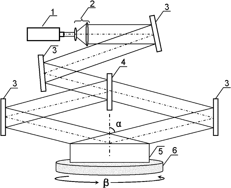
[0021] 3) Place the organic semiconductor thin film sample prepared above in the interference light path, such as figure 1 As shown, the angle 2α=44° between the two beams. A periodic one-dimensional organic semiconductor grating structure can be etched on the organic semiconductor film by manually triggering the laser to emit a laser pulse with an energy of 20mJ, a pulse width of 6ns, and a wavelength of 266nm.

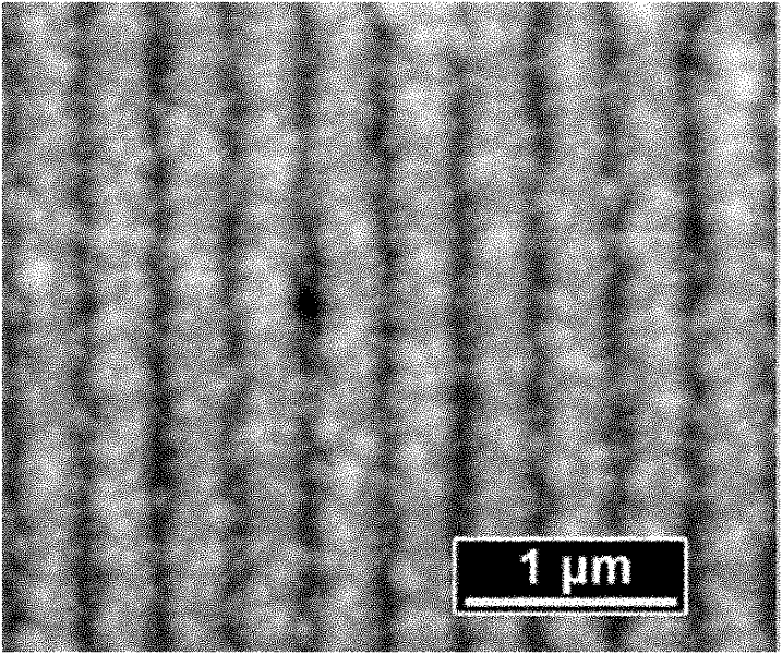
[0022] 4) The atomic force microscopy image of the structure of the prepared one-dimensiona...

Embodiment 2

[0023] Embodiment 2: Preparation of two-dimensional organic semiconductor nanostructure (two-dimensional square structure)

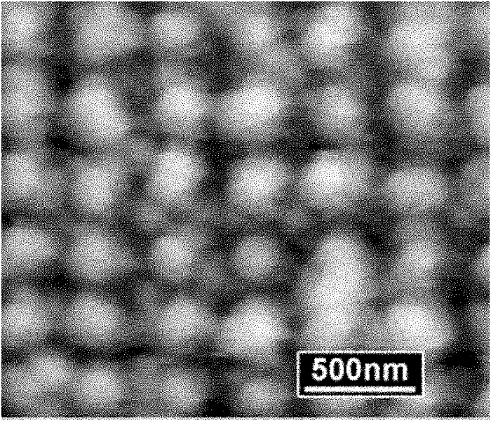
[0024] On the basis of the one-dimensional organic semiconductor grating preparation technology realized in Example 1, the sample is rotated by β=90° with the normal direction of the substrate plane as the axis, and then the second exposure and ablation are performed to realize the two-dimensional organic semiconductor grating. Preparation of semiconductor nanostructures, atomic force microscope (AFM) photos of two-dimensional organic semiconductor grating structures, see figure 2 .

Embodiment 3

[0025] Embodiment 3: Preparation of two-dimensional organic semiconductor nanostructure (two-dimensional triangular structure)

[0026] On the basis of the one-dimensional organic semiconductor grating preparation technology realized in Example 1, the sample is rotated by β=60° with the normal direction of the substrate plane as the axis, and then the second exposure and ablation are performed to realize the two-dimensional organic semiconductor grating. Preparation of semiconductor nanostructures.


PUM

PropertyMeasurementUnit
thicknessaaaaaaaaaa
wavelengthaaaaaaaaaa

Abstract

The invention discloses a method for directly writing an organic semiconductor laser by ultraviolet laser interferometry etching and belongs to the technical field of nano photoelectronic materials and devices. The method comprises the steps as follows: (1), preparing fluorescent emission organic semiconductor material organic solution; (2), spin-coating the fluorescent emission organic semiconductor solution on a substrate to obtain an organic semiconductor membrane with uniform thickness of 50-500 nanometers; and (3), enabling strong ultraviolet laser interference patterns to act with the organic semiconductor membrane, so that the organic semiconductor membrane in an interference bright strip area is etched instantly and the unexposed area is left. The method has the advantages of low cost, good repeatability, high preparation efficiency and controllable cycle, and can be used for preparing large-area one-dimensional or two-dimensional organic semiconductor lasers.

Description

technical field [0001] The invention belongs to the technical field of nano-optoelectronic materials and devices, and in particular relates to directly writing period-controllable one-dimensional and two-dimensional organic semiconductor lasers on organic semiconductor thin films by using an ultraviolet laser interference ablation method. Background technique [0002] Optically pumped organic semiconductor lasers are of great significance for the realization of new laser light sources and future electrically pumped organic semiconductor lasers. The distributed feedback structure is the best structure to realize optically pumped organic semiconductor lasers. At present, the manufacturing methods of the distributed feedback structure are basically based on ultraviolet light relief, nanoimprinting, electron beam etching, reactive ion beam etching technology and the like. However, these manufacturing methods have problems such as complex process, expensive preparation equipment...

Claims


Application Information

Patent Timeline
Patent Type & Authority Applications(China)
IPC IPC(8): B23K26/067B23K26/36B23K101/40B23K26/362
Inventor 张新平翟天瑞
Owner BEIJING UNIV OF TECH
Why Eureka
Try Eureka