Axial diode and fabrication method of axial diode with polyimide glue as protection glue layer

A technology of axial diodes and polyimide glue, applied in semiconductor/solid-state device manufacturing, electrical components, electric solid-state devices, etc., can solve problems such as low product qualification rate, low production efficiency, and affecting the electrical properties of workpieces, and achieve The method is reasonable, the production efficiency is high, and the effect of improving electrical performance

Active Publication Date: 2012-08-29
常州银河电器有限公司
View PDF5 Cites 13 Cited by
  • Summary
  • Abstract
  • Description
  • Claims
  • Application Information

AI Technical Summary

Problems solved by technology

This will also affect the electrical properties of the workpiece, resulting in low product yield and low production efficiency.

Method used


Image

  • Axial diode and fabrication method of axial diode with polyimide glue as protection glue layer
  • Axial diode and fabrication method of axial diode with polyimide glue as protection glue layer
  • Axial diode and fabrication method of axial diode with polyimide glue as protection glue layer

Examples


specific Embodiment approach 1

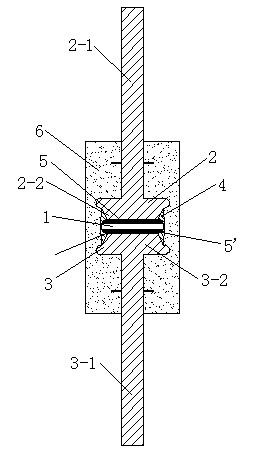
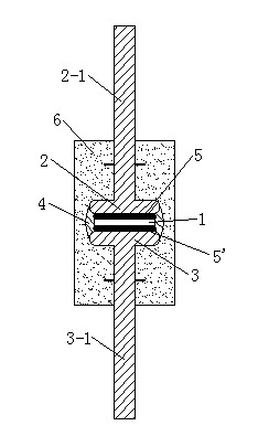
[0028] Such as figure 1 As shown, an axial diode includes a diode chip 1, a first copper electrode 2, a second copper electrode 3, a protective glue layer 4 and an epoxy insulating glue 6; the diode chip 1 is located between the first copper electrode 2 and the second copper electrode Between the two copper electrodes 3, and the positive and negative contact surfaces of the diode chip 1 are welded and connected to the first copper electrode 2 and the second copper electrode 3 respectively through the first soldering adhesive layer 5 and the second soldering adhesive layer 5' respectively. ; The first copper electrode 2 has a first lead 2-1 integrated with it, and the second copper electrode 3 has a second lead 3-1 integrated with it; and it: the first copper electrode 2 has a The first boss 2-2, the second copper electrode 3 has a second boss 3-2, the diode chip 1 is located between the first boss 2-2 and the second boss 3-2; the protective glue layer 4 Coated on the diode c...

specific Embodiment approach 2

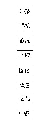
[0030] Such as figure 2 As shown, a method for preparing an axial diode whose protective adhesive layer is polyimide glue, the preparation method includes mounting, welding, pickling, gluing, curing, molding, aging and electroplating, and it:

[0031] a. The mounting step is to pack the first copper electrode 2, the first welding adhesion layer 5, the diode chip 1, the second welding adhesion layer 5' and the second copper electrode 3 into the graphite boat in sequence, and make it close together;

[0032] b. The welding step is to put the graphite boat into the welding furnace for structural welding, the time is within 6-10 minutes, and the temperature is controlled within the range of 300-360°C;

[0033]c, the pickling step is to put the workpiece after the welding step into the through hole of the pickling plate, then inject the mixed pickling solution into the working concave surface of the pickling plate to corrode the periphery of the diode chip 1, and the time is cont...


PUM

PropertyMeasurementUnit
purityaaaaaaaaaa

Abstract

The invention discloses an axial diode which comprises a diode chip, a first copper electrode, a second copper electrode, a protection glue layer and epoxy insulation glue, wherein the diode chip is located between the two copper electrodes; an anode contact surface and a cathode contact surface of the diode chip are respectively and integrally welded with the corresponding copper electrodes through a first welding adhesion layer and a second welding adhesion layer; the two copper electrodes are respectively provided with two leads that are integrated into a whole; each of the first copper electrode and the second copper electrode is provided with a boss; the diode chip is located between the two bosses; the protection glue layer is coated at the peripheries of the diode chip, the two bosses and the two welding adhesion layers; and the epoxy insulation glue is coated at the peripheries of the two copper electrodes, the protection glue layer and parts of the two leads. The fabrication method of the axial diode with the protection glue layer as polyimide glue comprises the steps of racking, welding, pickling, gluing, solidifying, mold pressing, aging and electroplating. The axial diode is good in electrical property and high in reliability; and the fabrication method has the characteristics that the fabrication method is more reasonable, and the production efficiency is high.

Description

technical field [0001] The invention relates to an axial diode and a preparation method thereof, belonging to the technical field of electronic semiconductor devices. Background technique [0002] At present, the existing axial diode is installed on the electronic circuit board through its lead wire, and plays a role of rectification. The protective glue included in the axial diode of this structure is silicon rubber. However, the silicone rubber is coated on the outer periphery of the diode chip, the first copper electrode, the second copper electrode, the first welding adhesive layer and the second welding adhesive layer, which can only play a role of sealing protection (as attached image 3 shown), but cannot absorb various ions remaining on the surface of the diode chip included in the workpiece after pickling during its preparation process. Detect the electrical properties of the workpiece in the range of 85~90%, and have a great influence on the electrical properties ...

Claims


Application Information

Patent Timeline
Patent Type & Authority Applications(China)
IPC IPC(8): H01L29/861H01L23/29H01L23/49H01L21/56
CPCH01L24/01H01L24/33H01L2224/01H01L2924/181H01L2924/00012
Inventor 朱伟英莫行晨
Owner 常州银河电器有限公司
Why Eureka
Try Eureka