OLED (organic light-emitting diode) device, AMOLED (active matrix organic light-emitting diode) device and manufacturing method of AMOLED device

A device and anode layer technology, which is applied in the field of lighting device and display device manufacturing, can solve the problems of complex manufacturing process and high production cost of AMOLED devices, achieve the effects of shortening production time, reducing manufacturing process, and improving luminous efficiency

Active Publication Date: 2012-08-29
BOE TECH GRP CO LTD
View PDF5 Cites 34 Cited by
  • Summary
  • Abstract
  • Description
  • Claims
  • Application Information

AI Technical Summary

Problems solved by technology

This complex structure causes the manufacturing process of AMOLED devices to be complicated and the production cost is high.

Method used


Image

  • OLED (organic light-emitting diode) device, AMOLED (active matrix organic light-emitting diode) device and manufacturing method of AMOLED device
  • OLED (organic light-emitting diode) device, AMOLED (active matrix organic light-emitting diode) device and manufacturing method of AMOLED device
  • OLED (organic light-emitting diode) device, AMOLED (active matrix organic light-emitting diode) device and manufacturing method of AMOLED device

Examples


no. 1 example

[0060] As the first embodiment of the manufacturing method of the AMOLED device provided by the present invention, as Figure 9 , the method includes the following steps,

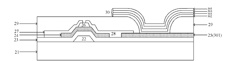
[0061] 501. Clean the substrate 21. SiO with a thickness of 200nm was deposited by CVD method 2 The thin film acts as a buffer layer. Metal Mo with a thickness of 200 nm is deposited by sputtering, and the gate electrode 22 is obtained by photolithography and etching. SiO with a thickness of 150 nm was deposited at 370 °C by CVD method 2 as the gate insulating layer 23 .

[0062] 502 . Deposit an IGZO film layer with a thickness of 50 nm by sputtering, and perform photolithography and etching to obtain the active layer 24 and the pixel electrode layer 25 .

[0063] 503. Deposit SiO with a thickness of 50 nm by sputtering 2 Layer, photolithography, etching to obtain the barrier layer 26.

[0064] 504. Deposit a metal layer with a thickness of 200 nm by using a sputtering method, where the metal layer ...

no. 3 example

[0079] As the third embodiment of the manufacturing method of the AMOLED device provided by the present invention, as Figure 11 , the method includes the following steps,

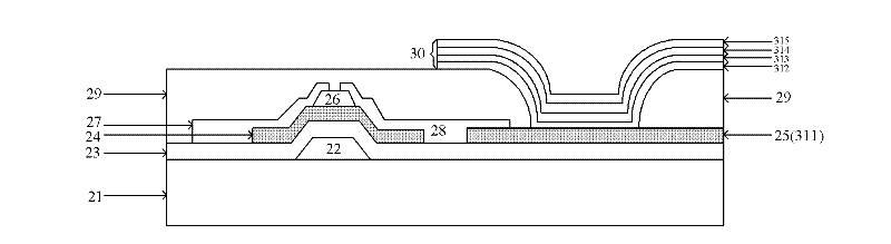
[0080] 701. Clean the substrate 21. An Al layer with a thickness of 150-300 nm is vapor-deposited on the back of the substrate 21 as a mirror. Metal Mo with a thickness of 200 nm is deposited by sputtering, and the gate electrode 22 is obtained by photolithography and etching. SiO with a thickness of 120 nm was deposited at 390 °C by CVD method 2 and SiN x as the gate insulating layer 23 .

[0081] 702. Deposit an IGZO thin film layer with a thickness of 50 nm by sputtering, and obtain the active layer 24 and the pixel electrode layer 25 by photolithography and etching.

[0082] 703. Deposit SiO with a thickness of 50 nm by sputtering 2 Layer, photolithography, etching to obtain the barrier layer 26.

[0083] 704. Deposit a metal layer with a thickness of 200 nm by using a sputtering method, where t...


PUM

PropertyMeasurementUnit
Deposition thicknessaaaaaaaaaa
Thicknessaaaaaaaaaa
Thicknessaaaaaaaaaa

Abstract

The embodiment of the invention discloses an OLED (organic light-emitting diode) device, an AMOLED (active matrix organic light-emitting diode) device and a manufacturing method of the AMOLED device, and belongs to the field of manufacturing lighting devices and display devices. According to the invention, an adjustment range of electrode work functions of the OLED device is enlarged, the light emitting efficiency of the OLED device is increased, the manufacturing process of the AMOLED device is reduced, and the production cost is reduced. The AMOLED device comprises a TFT (thin film transistor) active layer, a pixel electrode layer and the OLED device, wherein the OLED device comprises a cathode layer and a functional layer, and the pixel electrode layer is taken as an anode layer of the OLED device; or the OLED device comprises an anode layer and the functional layer, wherein the pixel electrode layer is taken as the cathode layer of the OLED device; and the TFT active layer and the pixel electrode layer are formed by the same IGZO (indium gallium zinc oxide) film through a composition technology. The embodiment of the invention is applicable to manufacturing the lighting devices and the display devices.

Description

technical field [0001] The invention relates to the field of manufacturing lighting devices and display devices, in particular to an OLED device, an AMOLED device and a method for manufacturing the AMOLED device. Background technique [0002] The basic structure of an organic light-emitting display device (Organic Light-Emitting Diode, OLED) includes an anode layer, a functional layer and a cathode layer. The functional layer includes: a hole transport layer, a light emitting layer and an electron transport layer. When an appropriate voltage is supplied to the cathode and anode, electrons and holes are injected from the cathode and anode into the electron and hole transport layer respectively, and migrate to the light-emitting layer through the electron and hole transport layer respectively, and the holes and electrons are in the light-emitting layer Composite light emission, so as to realize the characteristic of self-light emission of the OLED device. [0003] In order t...

Claims


Application Information

Patent Timeline
IPC IPC(8): H01L51/52H01L51/54H01L27/32H01L21/77
CPCH01L27/1225H10K59/123H10K50/81H10K50/828H10K50/856H10K2102/101H10K2102/321H10K2102/3031H10K59/1201H10K59/131H10K50/82H10K71/00
Inventor 李延钊王刚李禹奉张立
Owner BOE TECH GRP CO LTD
Why Eureka
Try Eureka