Manufacturing method for organic semiconductor laser based on active waveguide grating structure
A technology of organic semiconductor and grating structure, which is applied in the field of preparation of organic semiconductor lasers, can solve the problems of poor laser mode and uneven thickness of active material film, and achieve the effects of low cost, good laser mode and high production efficiency
- Summary
- Abstract
- Description
- Claims
- Application Information
AI Technical Summary
Problems solved by technology
Method used
Image

Examples
Embodiment 1
[0016] Embodiment 1: Preparation of a one-dimensional organic semiconductor laser based on an active waveguide (one-dimensional structure)
[0017] 1) Dissolving organic semiconductor F8BT in organic solvents such as toluene, xylene, chloroform, cyclohexane, pentane, hexane or octane, to prepare a F8BT organic semiconductor solution with a concentration of 15mg / ml;
[0018] 2) Spin-coat the F8BT organic semiconductor solution on the glass substrate. The spin coating speed is 1800rpm, and the corresponding film thickness is 150nm;
[0019] 3) The recording medium S1805 photoresist is spin-coated on the organic semiconductor thin film in step 2). The spin coating speed is 2000rpm, and the corresponding film thickness is 500nm;
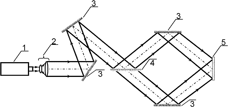
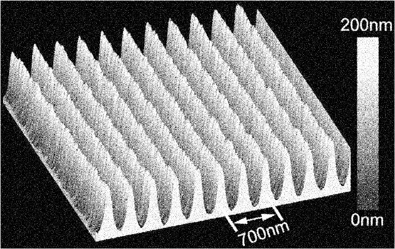
[0020] 4) Place the double-layer film sample prepared above in the interference light path, such as figure 1 As shown, among them, the wavelength of the laser used in interference lithography is 355nm, and the interference fringes can be recorded on t...
Embodiment 2
[0022] Example 2: Preparation of one-dimensional organic semiconductor laser based on active waveguide
[0023] 1) Dissolving the organic semiconductor F8BT in an organic solvent such as toluene, xylene, chloroform, cyclohexane, pentane, hexane or octane, to prepare a F8BT organic semiconductor solution with a concentration of 25mg / ml;
[0024] 2) Spin-coat the F8BT organic semiconductor solution on the glass substrate. The spin coating speed is 2000rpm, and the corresponding film thickness is 150nm;
[0025] 3) The recording medium S1805 photoresist is spin-coated on the organic semiconductor thin film in step 2). The spin coating speed is 2000rpm, and the corresponding film thickness is 500nm;
[0026] 4) Place the double-layer film sample prepared above in the interference light path, such as figure 1 As shown, among them, the wavelength of the laser used in interference lithography is 355nm, and the interference fringes can be recorded on the upper photoresist film, and...
Embodiment 3
[0027] Example 3: Preparation of one-dimensional organic semiconductor laser based on active waveguide
[0028] 1) Dissolving organic semiconductor PFB in organic solvents such as toluene, xylene, chloroform, cyclohexane, pentane, hexane or octane, to make a PFB organic semiconductor solution with a concentration of 15 mg / ml;
[0029] 2) Spin-coat the PFB organic semiconductor solution on the glass substrate. The spin coating speed is 1000rpm, and the corresponding film thickness is 200nm;
[0030] 3) The recording medium S1805 photoresist is spin-coated on the organic semiconductor thin film in step 2). The spin coating speed is 2000rpm, and the corresponding film thickness is 500nm;
[0031] 4) Place the double-layer film sample prepared above in the interference light path, such as figure 1 As shown, among them, the wavelength of the laser used in interference lithography is 355nm, and the interference fringes can be recorded on the upper photoresist film, and then the p...
PUM
| Property | Measurement | Unit |
|---|---|---|
| Thickness | aaaaa | aaaaa |
| Wavelength | aaaaa | aaaaa |
Abstract
Description
Claims
Application Information
 - Generate Ideas
- Intellectual Property
- Life Sciences
- Materials
- Tech Scout
- Unparalleled Data Quality
- Higher Quality Content
- 60% Fewer Hallucinations
Browse by: Latest US Patents, China's latest patents, Technical Efficacy Thesaurus, Application Domain, Technology Topic, Popular Technical Reports.
© 2025 PatSnap. All rights reserved.Legal|Privacy policy|Modern Slavery Act Transparency Statement|Sitemap|About US| Contact US: help@patsnap.com