

Method for manufacturing thin-film substrate
A thin-film substrate and manufacturing method technology, which is applied in the fields of film/sheet adhesive, printed circuit manufacturing, semiconductor/solid-state device manufacturing, etc., can solve problems such as inability to use TFT equipment, lower yield rate, and inability to use thin-film substrates , achieve the effect of efficient and stable pattern forming method, improve device operation rate, and cheap circuit components
- Summary
- Abstract
- Description
- Claims
- Application Information
AI Technical Summary
Problems solved by technology
Method used
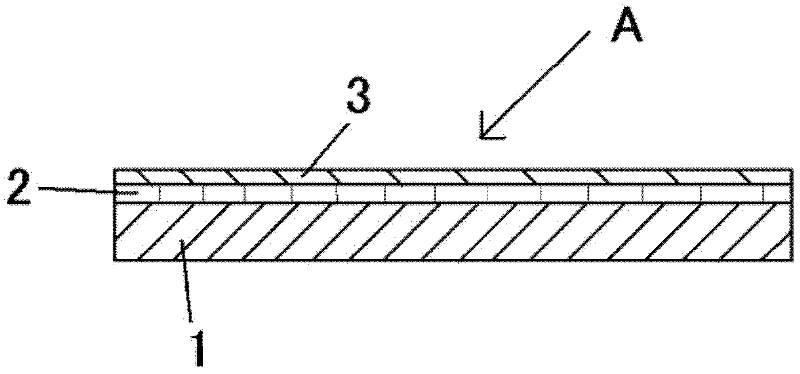
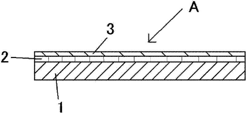
Image

Examples
Embodiment 1
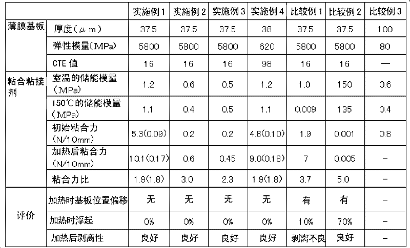
[0155] With respect to 60 moles of methoxyethyl acrylate, 22 moles of acryloylmorpholine and 16 moles of 2-hydroxyethyl acrylate were copolymerized in ethyl acetate by a conventional method. Addition reaction of the NCO group of 2-methacryloyloxyethylene isocyanate to 50% of the side chain terminal OH group of 2-hydroxyethyl acrylate to obtain a weight-average compound containing a carbon-carbon double bond at the end. A solution of an acrylic copolymer with a molecular weight of 900,000.
[0156] Next, with respect to 100 parts by weight of the solution containing the acrylic copolymer, 3 parts by weight of a photopolymerization initiator (trade name "IRGACURE 127", manufactured by BASF) and 3 parts by weight of a polyisocyanate compound (trade name "CORONATEL", manufactured by Japan Polyurethane Manufacturing), to obtain an acrylic ultraviolet curable adhesive solution.
[0157] This adhesive solution was coated on glass as a hard substrate, and heated and crosslinked at 12...
Embodiment 2
[0159] With respect to 100 parts by weight of 2-ethylhexyl acrylate, 10 parts by weight of 2-hydroxyethyl acrylate was copolymerized in ethyl acetate by a conventional method to obtain a solution containing an acrylic copolymer with a molecular weight of 800,000. Next, 5 parts by weight of a polyisocyanate compound (trade name "CORONATE L", manufactured by Nippon Polyurethane Co., Ltd.) was added to 100 parts by weight of the solution containing the acrylic copolymer to obtain an acrylic adhesive solution.
[0160] Using these adhesive solutions, an adhesive layer and a PET tape having a thickness of 30 μm were prepared under the same conditions as in Example 1.
Embodiment 3
[0162] With respect to 100 parts by weight of 2-ethylhexyl acrylate, 2 parts by weight of acrylic acid was copolymerized in ethyl acetate by a conventional method to obtain a solution containing an acrylic copolymer with a molecular weight of 500,000.
[0163] Next, 1 part by weight of an epoxy compound (trade name "TETRAD-C", manufactured by Mitsubishi Gas Chemical) was added to 100 parts by weight of the solution containing the acrylic copolymer to obtain an acrylic adhesive solution.
[0164] Using these adhesive solutions, an adhesive layer and a PET tape having a thickness of 30 μm were prepared under the same conditions as in Example 1.
PUM
| Property | Measurement | Unit |
|---|---|---|
| thickness | aaaaa | aaaaa |
| thickness | aaaaa | aaaaa |
| peel strength | aaaaa | aaaaa |
Abstract
Description
Claims
Application Information