Preparation method for ZnO/ZnS heterostructure nanocone array

A heterostructure and nano-cone technology, applied in the manufacture of discharge tubes/lamps, microstructure technology, microstructure devices, etc., can solve problems such as unsatisfactory field emission performance, high turn-on electric field and threshold electric field

Inactive Publication Date: 2012-09-12
HARBIN NORMAL UNIVERSITY
View PDF1 Cites 3 Cited by
  • Summary
  • Abstract
  • Description
  • Claims
  • Application Information

AI Technical Summary

Problems solved by technology

[0003] The present invention aims to solve the problem of unsatisfactory field emission performance due to the relatively high turn-on electric field and threshold electric field of nanomaterials with special morphology, and provides a preparation method for ZnO / ZnS heterostructure nanocone arrays

Method used


Image

  • Preparation method for ZnO/ZnS heterostructure nanocone array
  • Preparation method for ZnO/ZnS heterostructure nanocone array
  • Preparation method for ZnO/ZnS heterostructure nanocone array

Examples


specific Embodiment approach 1

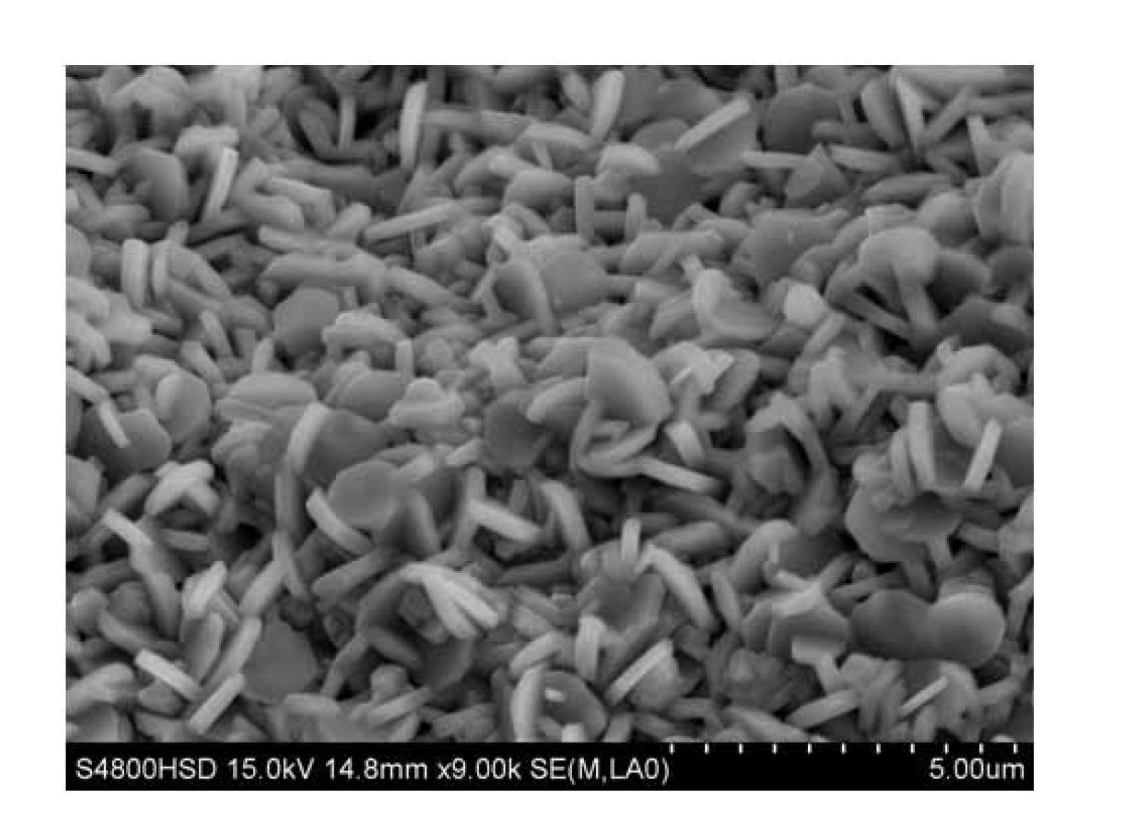
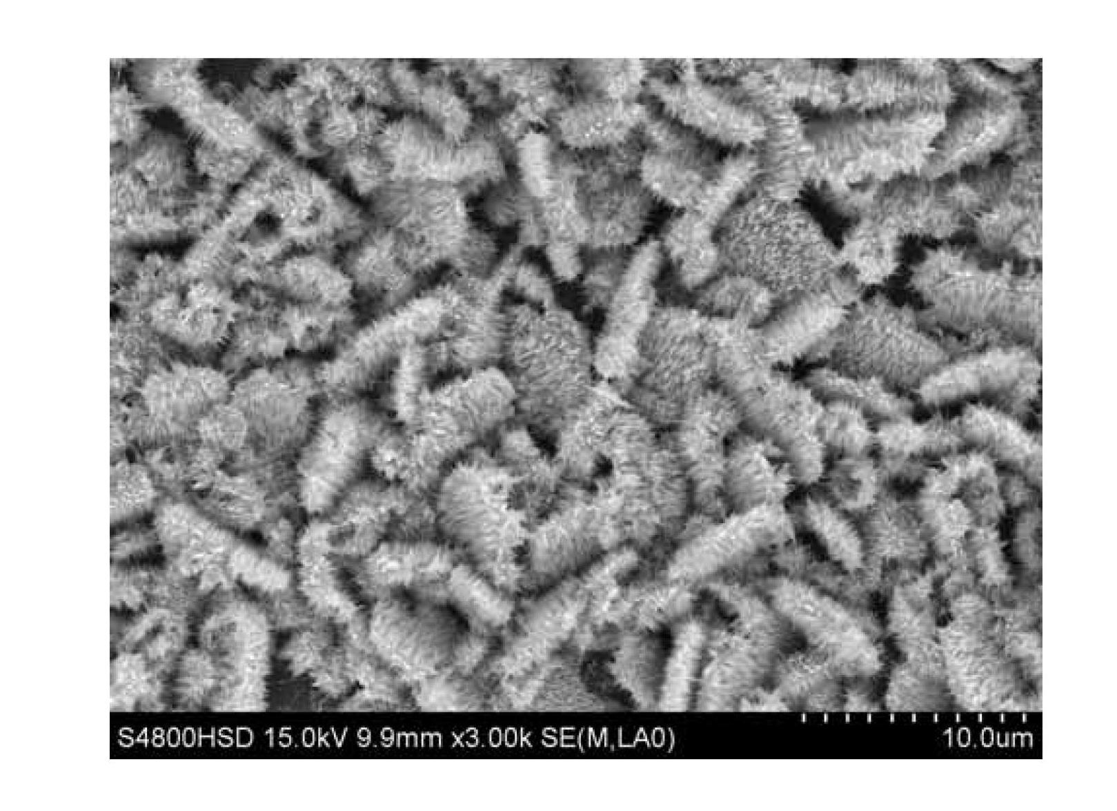
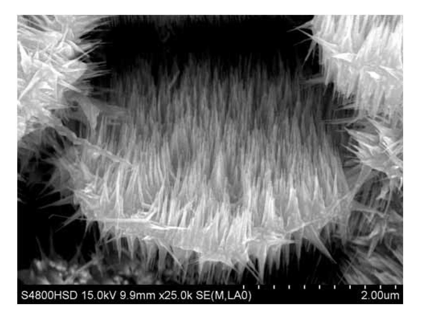
[0009] Specific embodiment one: the preparation method of the ZnO / ZnS heterostructure nanocone array of this embodiment is carried out according to the following steps: one, the single crystal silicon wafer is cleaned, and then the nano-gold film is sputtered on the single crystal silicon wafer as Silicon substrate; 2. Mix zinc oxide powder and zinc sulfide powder in a mass ratio of 1 to 25:1 as the source material, germanium powder as the catalyst, and place the source material, catalyst and silicon substrate in a high-temperature resistant container , where the source material is placed at one end of the high-temperature resistant container, and this end is placed at the center of the high-temperature reaction furnace, the catalyst is placed downstream of the source material, and the distance between the source material and the source material is 0.06-0.08m, and the silicon substrate Place it downstream of the source material, and the distance between it and the source materi...

specific Embodiment approach 2

[0010] Embodiment 2: This embodiment differs from Embodiment 1 in that: the single crystal silicon wafer in step 1 is n-type or p-type. Others are the same as in the first embodiment.

specific Embodiment approach 3

[0011] Specific embodiment three: the difference between this embodiment and specific embodiment one or two is: the process of cleaning the monocrystalline silicon wafer in step one is: first use acetone to ultrasonically clean for 15 minutes, then use absolute ethanol to ultrasonically clean for 15 minutes, and finally Ultrasonic cleaning with deionized water for 15 min. Others are the same as in the first or second embodiment.


PUM

PropertyMeasurementUnit
thicknessaaaaaaaaaa
lengthaaaaaaaaaa
diameteraaaaaaaaaa

Abstract

The invention relates to a preparation method for a ZnO/ZnS heterostructure nanocone array, and the method is used for solving the problem that the existing nanometer materials with a special appearance structure have higher turn-on field or threshold field to cause poor field emission property. The method comprises the following steps of: 1, cleaning a monocrystalline silicon slice, sputtering a nanometer gold film on the monocrystalline silicon slice so as to be used as a silicon substrate; 2, mixing zinc oxide powder and zinc sulfide powder so as to be used as a source material, taking germanium powder as a catalyst, placing the source material in a high temperature-resistant container and in a high-temperature reacting furnace, and placing the catalyst and the silicon substrate at the lower course of the source material; 3, sealing the high-temperature reacting furnace, vacuumizing, introducing inert gas, heating, keeping temperature constant, naturally cooling to the room temperature, stopping the introduction of the inert gas, and taking out the silicon substrate, thus obtaining yellowish white powder, namely the nanocone array. The nanocone array prepared by the invention has the advantages of extremely low turn-on field and extremely low threshold field; and the method is used for the field of nanometer materials.

Description

technical field [0001] The invention relates to a preparation method of a ZnO / ZnS heterostructure nano cone array. Background technique [0002] In recent years, with the development of science and technology, people have an increasing demand for high-tech equipment such as vacuum microwave amplifiers, flat panel displays and X-ray sources. In order to improve the commercial application value of these equipment, the research on the field emission properties of nanomaterials has attracted has attracted the great attention of many scientific researchers. However, how to improve the limited field emission performance is still a challenging problem. Generally speaking, optimizing geometrical factors and constructing nanomaterial arrays with novel structures can optimize the field emission performance of materials; on the other hand, field enhancement factor β is a very important characteristic parameter to measure field emission performance, which involves the Structure, shape...

Claims


Application Information

Patent Timeline
Patent Type & Authority Applications(China)
IPC IPC(8): H01J9/02B81C1/00
Inventor 张喜田陈美陆温静武立立牟洪臣
Owner HARBIN NORMAL UNIVERSITY
Why Eureka
Try Eureka