Array substrate and method for manufacturing polycrystalline silicon layer

A technology for array substrates and polysilicon layers, which is applied in transistors, semiconductor/solid-state device manufacturing, electrical components, etc., and can solve problems such as damaging flexible substrates, component degradation, and affecting the characteristics of display components

Active Publication Date: 2012-09-12
AU OPTRONICS CORP
View PDF4 Cites 13 Cited by
  • Summary
  • Abstract
  • Description
  • Claims
  • Application Information

AI Technical Summary

Problems solved by technology

In other words, the current low-temperature polysilicon manufacturing process may damage the properties of components such as flexible subst

Method used


Image

  • Array substrate and method for manufacturing polycrystalline silicon layer
  • Array substrate and method for manufacturing polycrystalline silicon layer
  • Array substrate and method for manufacturing polycrystalline silicon layer

Examples


Embodiment Construction

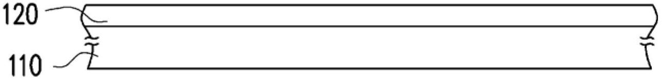
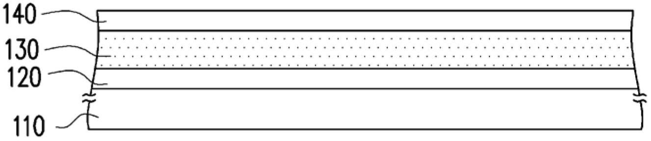
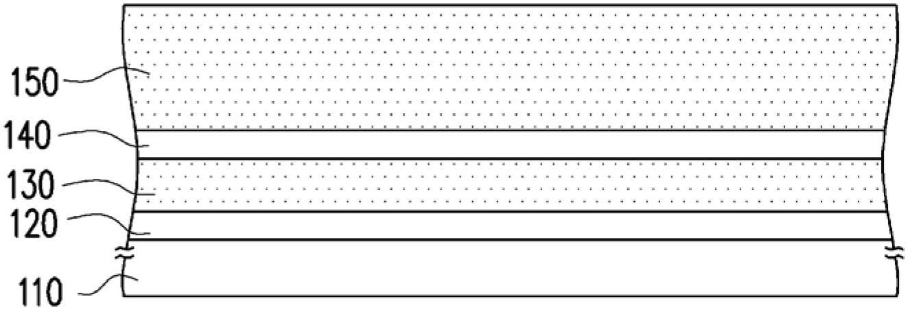
[0037] Figure 1A to Figure 1E is a schematic cross-sectional flow diagram of a method for fabricating a polysilicon layer according to an embodiment of the present invention. Please refer to Figure 1A Firstly, the first buffer layer 120 is formed on the flexible substrate 110 . In this embodiment, the flexible substrate 110 is, for example, a polyimide substrate, a glass substrate, a metal substrate or other substrates. The thickness of the flexible substrate 110 is, for example, greater than 0.01 mm. In one embodiment, the glass transition temperature of the flexible substrate 110 is, for example, less than 400°C. The material of the first buffer layer 120 is, for example, a dielectric material including silicon nitride, silicon oxide, or silicon oxynitride, and its thickness is, for example, 50 nm. A method for forming the first buffer layer 120 is, for example, plasma-assisted chemical vapor deposition.

[0038] Please refer to Figure 1B , and then, a first barrier ...


PUM

PropertyMeasurementUnit
Thermal conductivityaaaaaaaaaa
Thicknessaaaaaaaaaa
Thicknessaaaaaaaaaa

Abstract

The present invention discloses an array substrate and a method for manufacturing a polycrystalline silicon layer, wherein the method comprises the steps of forming a first buffer layer on a flexible layer, forming a first barrier layer on the first buffer layer, forming a second buffer layer on the first barrier layer, forming a second barrier layer on the second buffer layer, forming an amorphous silicon layer on the second barrier layer, and converting the amorphous silicon layer into the polycrystalline silicon layer through laser.

Description

technical field [0001] The invention relates to a manufacturing method of a substrate and a film layer, and in particular to a manufacturing method of an array substrate and a polysilicon layer. Background technique [0002] In recent years, with the increasing maturity of optoelectronic technology and semiconductor manufacturing technology, flat-panel displays have flourished. Among them, liquid crystal displays have gradually replaced traditional cathodes based on their advantages of low-voltage operation, no radiation scattering, light weight, and small size. Ray tube displays have become the mainstream of display products in recent years. Generally speaking, liquid crystal displays can be divided into two types: amorphous silicon thin film transistor liquid crystal display and low temperature poly-silicon thin film transistor liquid crystal display. [0003] Because low-temperature polysilicon thin film transistors have better device characteristics such as high carrier...

Claims


Application Information

Patent Timeline
IPC IPC(8): H01L29/786H01L21/336H01L21/20
Inventor 刘展睿李泓纬陈重嘉方俊雄
Owner AU OPTRONICS CORP
Why Eureka
Try Eureka