Clock generation circuit and analogue-to-digital converter (ADC) sampling circuit

A clock generation circuit and clock signal technology, applied in electrical components, electrical signal transmission systems, analog-to-digital converters, etc., can solve problems such as limited increase in clock signal voltage value, complex circuit structure, and variable on-resistance of transistor switches. , to achieve the effect of improving response speed, reducing harmonic distortion and small equivalent resistance

Active Publication Date: 2012-09-12
SHANGHAI HUAHONG GRACE SEMICON MFG CORP
View PDF5 Cites 4 Cited by
  • Summary
  • Abstract
  • Description
  • Claims
  • Application Information

AI Technical Summary

Problems solved by technology

[0010] The present invention solves the problem that the circuit structure of the clock generation circuit in the prior art is complex, and the

Method used


Image

  • Clock generation circuit and analogue-to-digital converter (ADC) sampling circuit
  • Clock generation circuit and analogue-to-digital converter (ADC) sampling circuit
  • Clock generation circuit and analogue-to-digital converter (ADC) sampling circuit

Examples


Example Embodiment

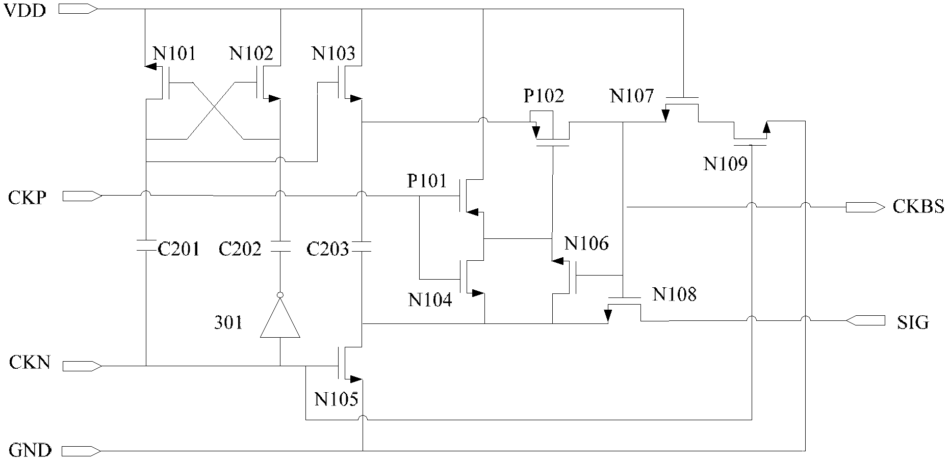
[0074] The working process of the clock generating circuit of the second embodiment is similar to that of the first embodiment, and will not be repeated here.
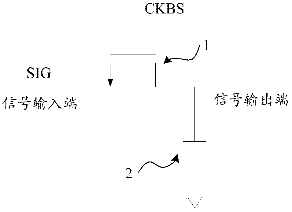
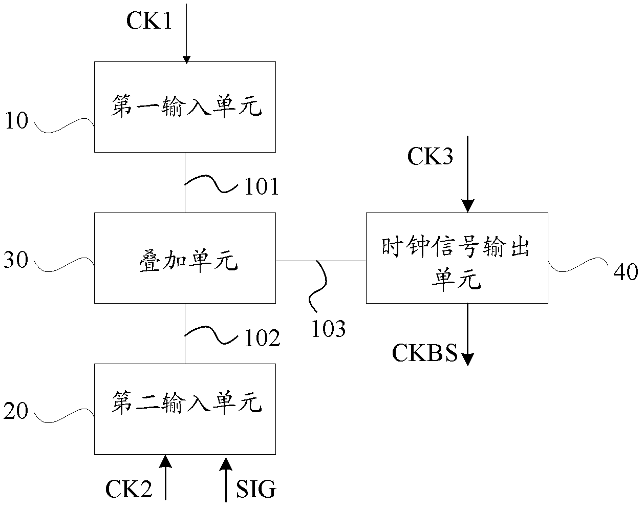
[0075] Figure 7 Shows a schematic diagram of the waveform of a clock signal generated by superimposing a voltage pulse signal and an analog pulse signal. by Figure 7 It can be seen that the voltage value of the clock signal CKBS is the sum of the power supply voltage of the bias power supply VDD and the voltage of the analog signal SIG. Combining the foregoing formula, for an NMOS transistor, the gate input clock signal CKBS, the source input analog signal SIG, so V g -V in Certainly, that is, the equivalent resistance R of the NMOS transistor switch is constant, and the NMOS transistor switch can be regarded as a constant conductance switch.

[0076] It should be noted that the first pulse control signal CK1, the second pulse control signal CK2, and the third pulse control signal CK3 can be based on the first input uni...


PUM


Abstract

The invention discloses a clock generation circuit and an analogue-to-digital converter (ADC) sampling circuit. The clock generation circuit comprises a first input unit, a second input unit, a superposition unit and a clock signal output unit, wherein the first input unit is used for providing a voltage pulse signal on the basis of a first pulse control signal; the second input unit is used for providing an analogue pulse signal on the basis of a second pulse control signal; the superposition unit is connected with the first and second input units, and is used for receiving the voltage pulse signal and the analogue pulse signal, and superposing the voltage pulse signal and the analogue pulse signal to generate a clock pulse signal; and the clock signal output unit is connected with the superposition unit, and is used for outputting a clock signal on the basis of a third pulse control signal. By the clock generation circuit, the output clock signal is associated with an analogue signal input by a sampling circuit, so that a difference between the gate voltage and source input voltage of a transistor switch in the sampling circuit is a constant value, and harmonic distortion is reduced.

Description

technical field [0001] The invention relates to the field of integrated circuits, in particular to a clock generation circuit and an ADC sampling circuit. Background technique [0002] With the development of contemporary microelectronics technology, an analog-to-digital converter (Analog-to-Digital Converter, ADC) as an analog and digital signal interface circuit has been widely used. Compared with other analog-to-digital converters, the pipeline ADC (pipeline ADC) has the advantages of high speed, high precision and low power consumption. [0003] The function of the pipeline analog-to-digital converter is to convert the input analog quantity into a digital quantity. The conversion process generally includes four steps of sampling, holding, quantization and encoding. In actual A / D conversion, sampling and holding are often combined. Sampling (also known as sampling or sampling) refers to periodically extracting the amplitude of the input analog signal at a certain freque...

Claims


Application Information

Patent Timeline
IPC IPC(8): H03M1/12H03M1/54
Inventor 秦义寿
Owner SHANGHAI HUAHONG GRACE SEMICON MFG CORP
Why Eureka
Try Eureka