

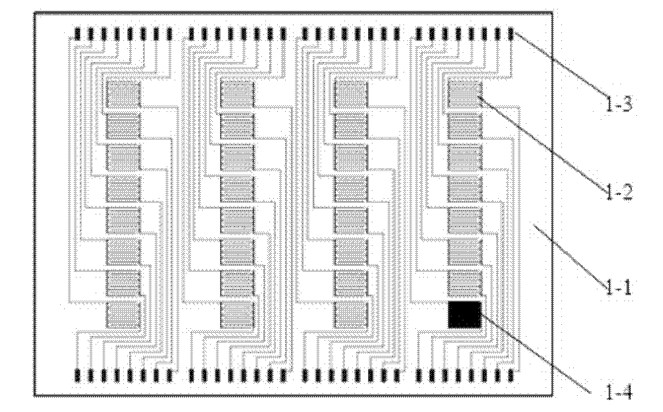
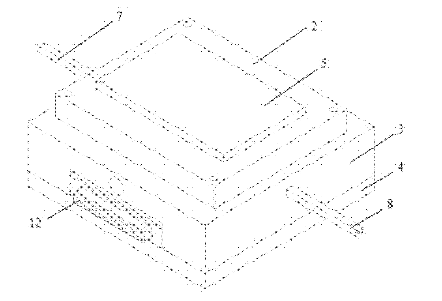
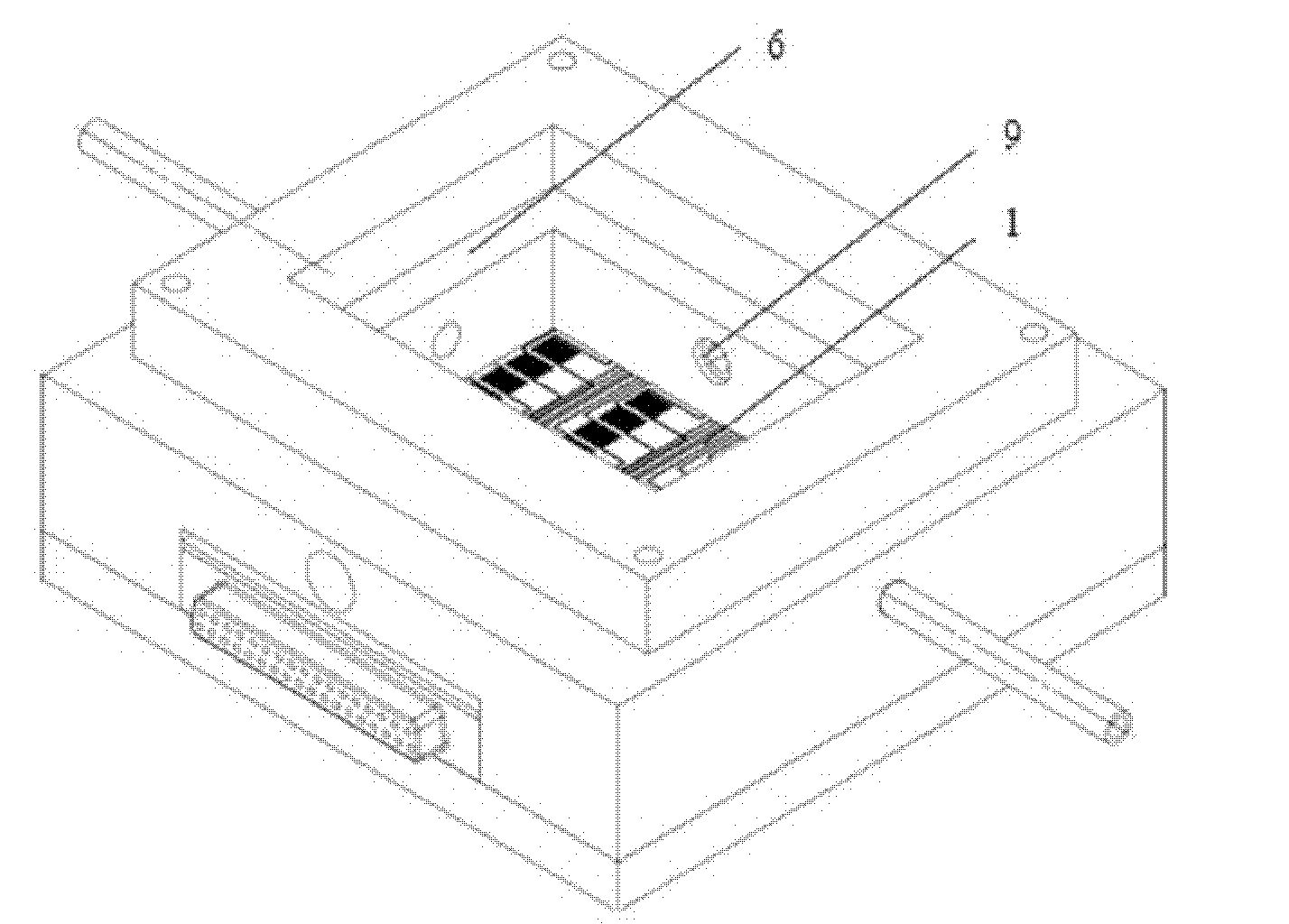
Chip and apparatus for high-flux testing gas-phase photoelectric properties of semiconductor
A photoelectric performance, semiconductor technology, applied in the direction of measuring devices, measuring electrical variables, measuring current/voltage, etc., to achieve the effect of simple preparation method, high integration and good controllability
- Summary
- Abstract
- Description
- Claims
- Application Information
AI Technical Summary
Problems solved by technology
Method used
Image

Examples
example 1
[0027] Adopt the miniature high-throughput gas-phase photoelectric performance comprehensive testing device provided by the invention to TiO 2 / ZnO / Fe 2 o 3 The composite system was screened for photoelectric properties. In this composite material system, a total of 66 composition points were selected, as shown in Table 1:
[0028] Table 1 TiO 2 / ZnO / Fe 2 o 3 Correspondence between ingredients and serial numbers in composite systems
[0029]
[0030]
[0031] At room temperature, keep the dry air circulating inside the device, and under the condition of an applied bias voltage of 0.2V, the results of high-throughput photoelectric performance detection of these 66 component points are as follows: Figure 5 shown. The results showed that TiO 2 / ZnO / Fe 2 o 3 When the composite material system is 1:9:0, in blue light (475nm, 80.8W / m 2) under the irradiation, has the best photoelectric performance.
[0032] It can be seen that, in this example, the comprehensive t...
PUM
 Abstract
Description
Claims
Application Information