Raman spectrum high electromagnetic enhancement substrate coated with gain medium and preparation

A gain medium and Raman spectroscopy technology, applied in the field of molecular sensing, can solve the problems of low detection sensitivity and hinder the increase of SERS enhancement factor, and achieve the effect of improving practicability and compensating for metal loss.

Inactive Publication Date: 2012-09-19
NANKAI UNIV
View PDF2 Cites 9 Cited by
  • Summary
  • Abstract
  • Description
  • Claims
  • Application Information

AI Technical Summary

Problems solved by technology

However, Raman spectroscopy has a very fatal shortcoming: the detection sensitivity is too low, and the Raman scattering cross section of molecules is usually only 10 -29 cm -2 S -1 , so there are very high requirements for sample volume and spectrum acquisition time
Although the metal micro-nano substrate can greatly enhance the SERS signal, the further increase of the SERS enhancement factor based on the electromagnetic enhancement mechanism is hindered due to the existence of metal loss.

Method used


Image

  • Raman spectrum high electromagnetic enhancement substrate coated with gain medium and preparation
  • Raman spectrum high electromagnetic enhancement substrate coated with gain medium and preparation
  • Raman spectrum high electromagnetic enhancement substrate coated with gain medium and preparation

Examples


Embodiment

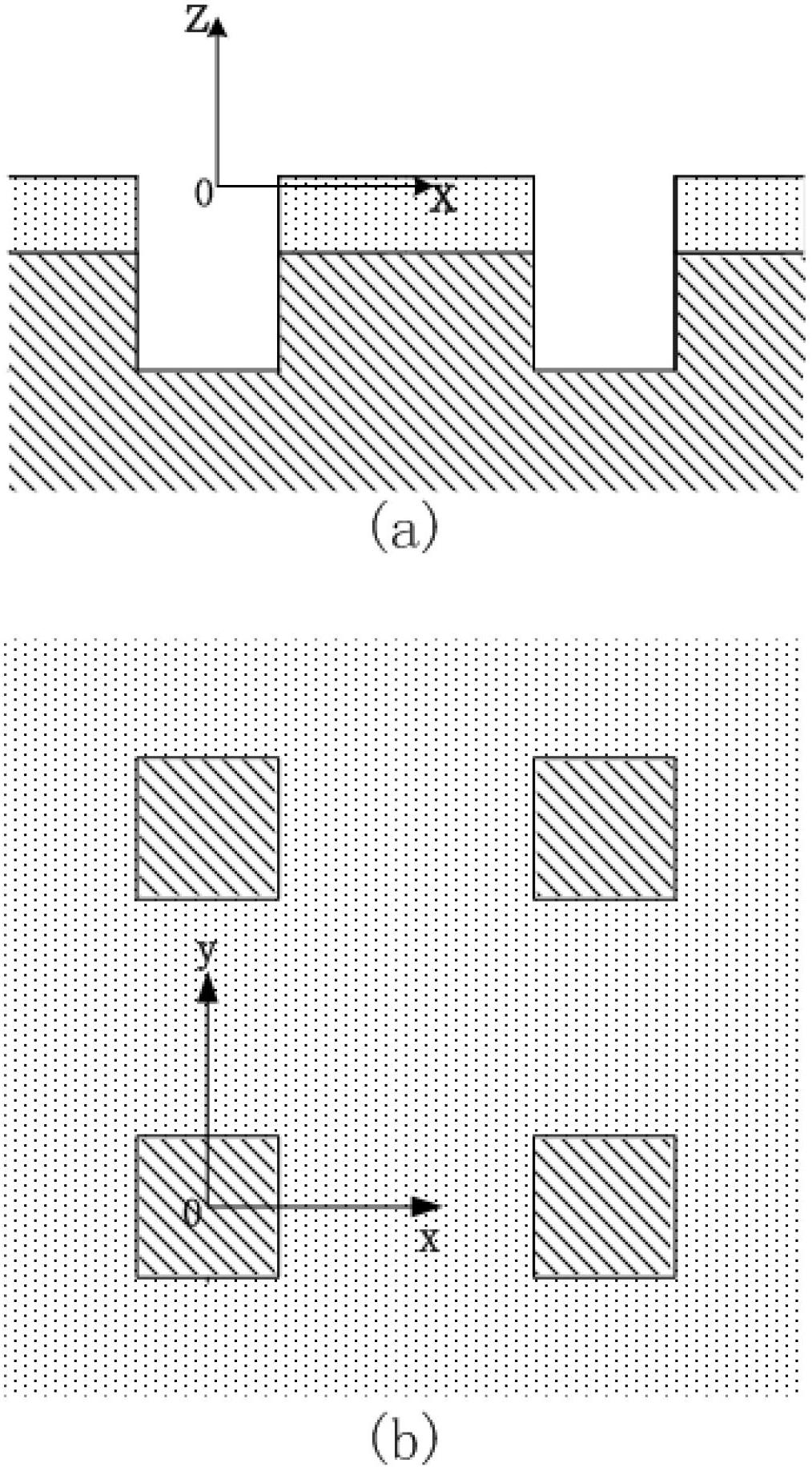
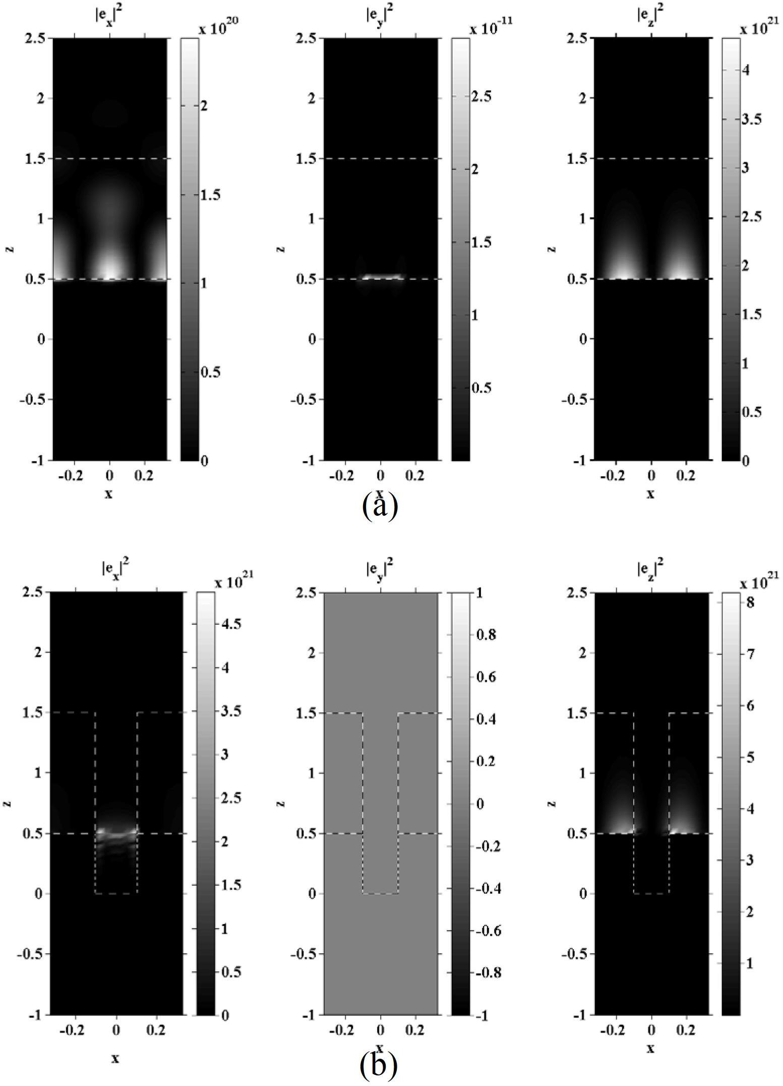
[0024] A Raman spectrum high electromagnetic enhancement substrate coated with a gain medium is a surface-enhanced Raman spectrum substrate structure coated with a gain medium on the surface of a metal blind hole array, such as figure 1 As shown, the pure gold film is used as the base metal, and the thickness of the gold film is 1 μm. There are square blind hole arrays evenly distributed on the base metal. The size of the blind holes in the blind hole array is 0.2 μm×0.2 μm, and the hole depth is 0.5 μm. The x-direction period is 0.65 μm and the y-direction period is 0.6 μm. The gain medium coated on the metal substrate is rhodamine 6G / polymethyl methacrylate (R6G / PMMA) film, and the thickness of the R6G / PMMA film is 1 μm.

[0025] The preparation of the Raman spectrum high electromagnetic enhancement substrate coated with the gain medium, the steps are as follows:

[0026] 1) Use 40mm×40mm×5mm ultraviolet optical quartz glass as the substrate, and use electron beam heating ev...


PUM

PropertyMeasurementUnit
sizeaaaaaaaaaa
thicknessaaaaaaaaaa
thicknessaaaaaaaaaa

Abstract

The invention relates to a Raman spectrum high electromagnetic enhancement substrate coated with a gain medium, which is an enhancement Raman spectrum substrate structure on a surface coated with gain medium on a metal blind hole array surface, wherein round, rectangular or triangular blind hole arrays are uniformly distributed on substrate metal, and the coated gain medium is a rhodamine6G/polymethylmethacrylate film which is prepared by dissolving dye molecules in an organic solvent. The preparation comprises the following steps of: dissolving rhodamine6G and polymethylmethacrylate into dichloromethane; then coating the obtained solution on the surface of a substrate metal chromium film and drying to form a film coated with the gain medium on the surface of the substrate metal chromium film; and processing blind hole arrays on the surface of the film by adopting a focused ion beam lithograplay technology. The Raman spectrum high electromagnetic enhancement substrate has the advantages that the gain medium material is introduced onto a traditional SERS (Surface Enhanced Raman Scattering) substrate to compensate metal loss so as to obtain SERS enhancement factors far higher than that of a substrate without a gain medium substrate, so that the practicality of the SERS is further improved, and a technical reference is provided for the research of SERS enhancement mechanism.

Description

technical field [0001] The invention belongs to the technical field of molecular sensing, and in particular relates to a Raman spectrum high electromagnetic enhancement substrate coated with a gain medium. Background technique [0002] The Raman scattering spectrum of molecules is directly related to the rotation and vibration of molecules, and can study the structure of matter at the molecular level. Food safety, inkblot identification, etc., have been more and more important applications. However, Raman spectroscopy has a very fatal shortcoming: the detection sensitivity is too low, and the Raman scattering cross section of molecules is usually only 10 -29 cm -2 S -1 , so there are very high requirements for sample volume and spectrum acquisition time. This limits the application of Raman spectroscopy to some extent. [0003] In 1974, M. Fleischmann et al. found for the first time in experiments that the Raman signal intensity of pyridine molecules adsorbed on the ele...

Claims


Application Information

Patent Timeline
Patent Type & Authority Applications(China)
IPC IPC(8): G01N21/65
Inventor 刘海涛张鑫
Owner NANKAI UNIV
Why Eureka
Try Eureka