Manufacture method of flip chip single-faced three-dimensional circuit manufactured by encapsulation prior to etching and flip chip single-faced three-dimensional circuit encapsulation structure

A three-dimensional circuit, sealing first and then etching technology, which is applied in semiconductor/solid-state device manufacturing, circuits, semiconductor/solid-state device components, etc., can solve the problems of great difference in material characteristics, stress deformation, and reliability that affect reliability and safety capabilities. Level and other issues, to achieve the effects of not being easily deformed by stress, reducing environmental pollution, and improving safety

Active Publication Date: 2013-09-04
JCET GROUP CO LTD
View PDF4 Cites 0 Cited by
  • Summary
  • Abstract
  • Description
  • Claims
  • Application Information

AI Technical Summary

Problems solved by technology

[0019]3. Glass fiber itself is a kind of foaming material, so it is easy to absorb moisture and moisture due to the storage time and environment, which directly affects the reliability and safety ability or is the level of reliability;
[0020] 4. The surface of the glass fiber is covered with a copper foil metal layer thickness of about 50-100 μm, and the etching distance between the metal layer line and the line can only achieve an etching gap of 50-100 μm due to the characteristics of the etching factor (see Figure 65 , the best production capacity is that the etching gap is approximately equal to the thickness of the etched object), so it is impossible to truly design and manufacture high-density circuits;
[0022]6. Also because the entire substrate material is made of glass fiber, the thickness of the glass fiber layer is obviously increased by 100~150μm, and it cannot be really ultra-thin encapsulation;
[0023]7. Due to the large difference in material characteristics (expansion coefficient) of the traditional glass fiber plus copper foil technology, it is easy to cause stress deformation in the harsh environment process, directly Affects the accuracy of component loading and the adhesion and reliability of components and substrates

Method used


Image

  • Manufacture method of flip chip single-faced three-dimensional circuit manufactured by encapsulation prior to etching and flip chip single-faced three-dimensional circuit encapsulation structure
  • Manufacture method of flip chip single-faced three-dimensional circuit manufactured by encapsulation prior to etching and flip chip single-faced three-dimensional circuit encapsulation structure
  • Manufacture method of flip chip single-faced three-dimensional circuit manufactured by encapsulation prior to etching and flip chip single-faced three-dimensional circuit encapsulation structure

Examples


Embodiment 1

[0109] Embodiment 1, no base island

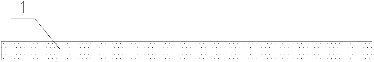
[0110] Step 1. Take the metal substrate

[0111] see figure 1 , take a metal substrate with a suitable thickness, the material of the metal substrate can be changed according to the function and characteristics of the chip, for example: copper, iron, nickel-iron or zinc-iron;

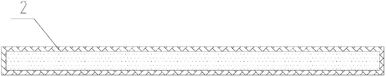
[0112] Step 2. Pre-plating copper on the surface of the metal substrate

[0113] see figure 2 , electroplating a layer of copper film on the surface of the metal substrate, the purpose is to serve as a basis for subsequent electroplating, and the electroplating method can be electroless plating or electrolytic plating;

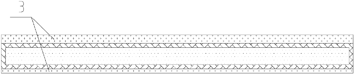
[0114] Step 3, green paint coating

[0115] see image 3 In step 2, the front and back of the metal substrate of the pre-plated copper film are covered with green paint to protect the subsequent electroplating metal layer process operations;

[0116] Step 4. Remove part of the green paint from the front of the metal substrate

[0117] see ...

Embodiment 2

[0162] Embodiment 2, there is base island

[0163] Step 1. Take the metal substrate

[0164] see Figure 27 , take a metal substrate with a suitable thickness, the material of the metal substrate can be changed according to the function and characteristics of the chip, for example: copper, iron, nickel-iron or zinc-iron;

[0165] Step 2. Pre-plating copper on the surface of the metal substrate

[0166] see Figure 28 , electroplating a layer of copper film on the surface of the metal substrate, the purpose is to serve as a basis for subsequent electroplating, and the electroplating method can be electroless plating or electrolytic plating;

[0167] Step 3, green paint coating

[0168] see Figure 29 In step 2, the front and back of the metal substrate of the pre-plated copper film are covered with green paint to protect the subsequent electroplating metal layer process;

[0169] Step 4. Remove part of the green paint from the front of the metal substrate

[0170] see ...


PUM

PropertyMeasurementUnit
thicknessaaaaaaaaaa

Abstract

The invention relates to a flip chip single-faced three-dimensional circuit manufacture method by encapsulation prior to etching. The method includes: taking a metal substrate; preplating copper to the metal substrate surface; coating with green paint; partially removing the green paint on the front of the metal substrate; electroplating an inert metal circuit layer; electroplating a metal circuit layer; coating with green paint; partially removing the green paint on the front of the metal substrate; electroplating metal circuit layer; coating with green paint; partially removing the green paint on the front of the metal substrate; coating a circuit screen plate; performing metallization pretreatment; removing the circuit screen plate; electroplating a metal circuit layer; mounting a chip and filling the bottom of the chip; encapsulating; partially removing the green paint on the back of the metal substrate; performing chemical etching; electroplating a metal circuit layer; coating with green paint; reserving holes on the green paint; cleaning; attaching balls; and cutting finished products. The flip chip single-faced three-dimensional circuit manufacture method by encapsulation prior to etching has the advantages that manufacture cost is lowered, safety and reliability of encapsulation are enhanced, environmental pollution is reduced, and design and manufacture of high density circuit are really achieved.

Description

technical field [0001] The invention relates to a chip flip-chip single-sided three-dimensional circuit manufacturing method which is first sealed and then etched and its packaging structure, which belongs to the technical field of semiconductor packaging. Background technique [0002] The manufacturing process flow of the traditional high-density substrate package structure is as follows: [0003] Step 1, see Figure 53 , take a substrate made of glass fiber material, [0004] Step two, see Figure 54 , opening holes at desired locations on the fiberglass substrate, [0005] Step three, see Figure 55 , coated with a layer of copper foil on the back of the glass fiber substrate, [0006] Step 4, see Figure 56 , fill the conductive material in the position where the glass fiber substrate is punched, [0007] Step five, see Figure 57 , coated with a layer of copper foil on the front of the glass fiber substrate, [0008] Step six, see Figure 58 , coated with a pho...

Claims


Application Information

Patent Timeline
Patent Type & Authority Patents(China)
IPC IPC(8): H01L21/48H01L21/56H01L23/31C25D5/10C25D5/02C25D7/00
CPCH01L24/97H01L2224/16225H01L2224/73204H01L2924/15311H01L21/48
Inventor 王新潮李维平梁志忠
Owner JCET GROUP CO LTD
Why Eureka
Try Eureka